Computer Architecture Assignment
Question 1. Write down the history of computer architecture over last 30 years.
Answer:
History of Computer Architecture Over the Last 30 Years
The evolution of computer architecture over the past three decades can be broadly divided into three major eras, shifting focus from pure raw speed to parallel processing, and finally to specialized, energy-efficient silicon.
The 1990s: The Frequency and Instruction-Level Parallelism (ILP) Race
During this decade, performance scaling was governed primarily by Dennard scaling and Moore’s Law. Clock frequencies doubled roughly every 18 months, leading to intense competition between manufacturers to reach higher gigahertz targets.
- Microarchitectures heavily exploited Instruction-Level Parallelism (ILP) using techniques like deep pipelining, out-of-order execution, branch prediction, and superscalar execution.
- The Reduced Instruction Set Computer (RISC) philosophy matured significantly, influencing mainstream architectures.
- Intel introduced iconic architectures like the Pentium Pro, Pentium II, and Pentium III, which brought advanced superscalar execution and dynamic execution to x86 processors.
The 2000s: The Power Wall and the Shift to Multi-Core
By the mid-2000s, the industry hit a major barrier known as the Power Wall. Increasing clock frequencies further resulted in unsustainable power consumption and heat dissipation, effectively ending the pure frequency race.
- Because single-threaded performance scaling hit a plateau, architects shifted their paradigm from making a single core run faster to putting multiple execution cores on a single silicon die.
- This birthed the Thread-Level Parallelism (TLP) era, making dual-core and quad-core processors standard for consumers and multi-socket, highly core-dense processors standard for servers.
- Memory latency also lagged severely behind processing speeds, leading to the Memory Wall. This forced architects to implement larger, multi-level cache hierarchies (L1, L2, and L3 caches) to minimize memory access bottlenecks.
The 2010s to Present: Amdahl's Law and Domain-Specific Architectures (DSAs)
As the physical limits of silicon fabrication approached (marking the slowing down of Moore’s Law), general-purpose CPUs could no longer deliver historic generational leaps in efficiency and speed.
- Architects increasingly turned to Heterogeneous Computing, combining different types of processing cores optimized for specific tasks on a single chip or System-on-Chip (SoC).
- The rise of big data, computer vision, and deep learning led to the proliferation of Domain-Specific Architectures (DSAs). Processing shifted toward highly parallel accelerators like Graphics Processing Units (GPUs) and Tensor Processing Units (TPUs) to bypass the limitations of general-purpose CPUs.
- Energy efficiency became the primary design constraint. This era saw the massive dominance of ARM-based architectures in mobile devices and their successful expansion into laptops (e.g., Apple’s M-series chips) and cloud data centers due to their superior performance-per-watt efficiency.
Question 2. Write down the classes of computer architecture.
Answer:
Classes of Computer Architecture:
Computer architecture can be classified based on how instructions and data are handled and organized. The main classes are:
1. Instruction Set Architecture (ISA)
This defines the programmer-visible part of the machine: instruction formats, opcodes, addressing modes, registers, and data types. Based on ISA design philosophy, architectures split into:
- CISC (Complex Instruction Set Computer) — e.g., x86, VAX
- RISC (Reduced Instruction Set Computer) — e.g., MIPS, ARM
- VLIW (Very Long Instruction Word) — multiple operations packed into one instruction
2. Flynn's Classification (based on instruction/data streams)
- SISD — Single Instruction, Single Data (traditional uniprocessor)
- SIMD — Single Instruction, Multiple Data (vector/array processors, GPUs)
- MISD — Multiple Instruction, Single Data (rare, e.g., fault-tolerant systems)
- MIMD — Multiple Instruction, Multiple Data (multiprocessors, multicore systems)
- SPMD — Single Program, Multiple Data (a software model, not pure hardware class — multiple processors run the same program independently on different data)
3. Micro-architecture Classification
- Single-cycle architecture
- Multi-cycle architecture
- Pipelined architecture
- Superscalar architecture (multiple instructions issued per cycle)
- Out-of-order execution architecture
4. Memory Architecture Classification
- Von Neumann architecture — single shared memory for instructions and data
- Harvard architecture — separate memory/buses for instructions and data
5. Based on Processing Approach
- Uniprocessor systems
- Multiprocessor systems (shared memory / distributed memory)
- Parallel processing architectures (array processors, vector processors, multicore)
Q3. What are the layers of computing system architecture?
Answer:
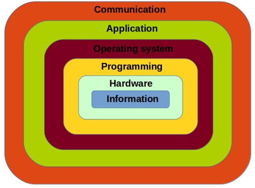
A computing system is organized as a hierarchy of layers, where each layer provides an abstraction to the layer above it while hiding the implementation details of the layers below it. This layered structure allows programmers, compiler designers, and hardware engineers to work independently at their own level without needing to understand the full depth of the system. There are seven such layers, arranged from the most abstract to the most physical.
Software Layers
At the top of the hierarchy lies the Application Software layer, consisting of programs used directly by end users, such as word processors, browsers, and games, typically written in high-level languages like C, Java, or Python.
Below this is the System Software layer, which has two important components. The Compiler translates the high-level language program into assembly instructions specific to a given machine's instruction set, while the Operating System manages hardware resources and provides essential services such as input-output handling, memory management, process scheduling, and file management, acting as an intermediary between application programs and the underlying hardware.
ISA and Microarchitecture Layers
Beneath the system software lies the Instruction Set Architecture (ISA) layer, which forms the interface between software and hardware. It defines the complete set of instructions a processor can execute, along with the registers, addressing modes, and data types available to the programmer. The compiler generates code targeting this layer, and it remains consistent even when the underlying hardware implementation changes. MIPS and x86 are common examples of ISAs.
Below the ISA lies the Microarchitecture layer, also called the Organization layer, representing the actual hardware implementation of a given ISA. This includes the data path, control unit, pipeline structure, and cache hierarchy. Two different processors can implement the same ISA yet have entirely different microarchitectures, resulting in different performance and power characteristics, as seen when comparing Intel and AMD processors that both implement the x86 ISA.
Hardware Realization Layers
Underneath the microarchitecture is the Logic Design layer, where digital circuits such as logic gates, flip-flops, multiplexers, and arithmetic logic units are designed using combinational and sequential logic principles to realize the microarchitecture.
Further down lies the Circuit layer, which deals with the transistor-level implementation of these logic gates, accounting for analog electrical properties such as voltage levels, current flow, and timing delays.
Finally, at the base is the Device or Physical layer, concerning the actual semiconductor devices and the physical fabrication process of the chip, involving silicon wafers, doping, and photolithography techniques. This is the domain of physics and materials science rather than computer science proper.
Together, these seven layers, namely Application Software, System Software, Instruction Set Architecture, Microarchitecture, Logic Design, Circuit Design, and Physical Devices, form a complete abstraction hierarchy. Each layer interacts only with its immediate neighboring layers, which is precisely what makes the design, understanding, and maintenance of modern computing systems practically feasible despite their enormous complexity.
Q4. What are the differences between RISC and CISC architecture?
Introduction
RISC (Reduced Instruction Set Computer) and CISC (Complex Instruction Set Computer) represent two contrasting philosophies of instruction set design. RISC architectures, such as MIPS and ARM, are built around a small set of simple, fixed-length instructions that execute in a single clock cycle, whereas CISC architectures, such as x86, provide a large set of complex, variable-length instructions capable of performing multi-step operations within a single instruction.
Instruction Set Complexity
In CISC design, instructions are complex and can perform multiple low-level operations, such as loading from memory, performing an arithmetic operation, and storing the result, all within a single instruction. This reduces the number of instructions per program but makes each instruction more complicated to decode and execute. In RISC design, each instruction performs only one simple operation, so more instructions are needed to accomplish the same task, but each individual instruction is straightforward to execute.
Instruction Format and Length
CISC instructions are typically of variable length, since different instructions require different amounts of encoding depending on their complexity and addressing mode. RISC instructions, in contrast, are of fixed length, usually one word (32 bits), which greatly simplifies instruction fetching and decoding in hardware.
Addressing Modes and Registers
CISC architectures support a large number of complex addressing modes, allowing operands to be accessed directly from memory in many different ways, and consequently tend to use fewer general-purpose registers since operations can be performed directly on memory. RISC architectures support only a few simple addressing modes and rely on a larger set of general-purpose registers for register-to-register operations, with memory accessed only through explicit load and store instructions, following what is known as a load-store architecture.
Execution Model and Performance
CPU performance for both approaches can be expressed using the fundamental CPU time equation:
This equation has three factors: the number of instructions required to execute the program, the average number of clock cycles needed per instruction (CPI), and the clock cycle time (the inverse of clock frequency). The two design philosophies attack this equation from opposite ends.
RISC reduces the cycles per instruction, at the cost of increasing the number of instructions per program:
CISC reduces the number of instructions per program, at the cost of increasing the number of cycles required per instruction:
For example, to add two 8-bit numbers, a CISC machine would use a single ADD instruction that internally handles the entire operation. A RISC machine would instead break the same task into separate load, operate, and store instructions:
As a result, RISC programs tend to be longer and require more memory to store, but the individual instructions are less complex and need fewer transistors to implement.
Hardware Design
CISC processors require a more complex control unit, often implemented using microcode, to decode and execute the wide variety of instructions, which also makes pipelining more difficult. RISC processors use simpler, hardwired control logic, since the instruction set itself is limited and uniform, which reduces hardware complexity and makes pipelining much easier to implement efficiently.
Historical Context
CISC architecture evolved during the era when programs were written directly in assembly language, where it was desirable for a single instruction to accomplish more work, since assembly programming was slow and error-prone. As high-level languages and compilers became dominant, the burden of translating operations shifted from the programmer to the compiler, which reduced the need for complex instructions and allowed the simpler RISC approach to become more practical and widely adopted.
Comparison Table
| Feature | RISC | CISC |
|---|---|---|
| Instruction set | Small and simple | Large and complex |
| Instruction length | Fixed | Variable |
| Cycles per instruction | Usually 1 | Multiple |
| Registers | More general-purpose registers | Fewer registers |
| Addressing modes | Simple and limited | Complex and many |
| Code size | Larger (more instructions) | Smaller (fewer instructions) |
| Hardware/pipelining | Simple hardware, easier pipelining | Complex hardware, harder pipelining |
| Examples | ARM, RISC-V, MIPS | x86, Intel 80386 |
In essence, CISC trades hardware simplicity at the compiler level for complexity at the processor level, while RISC does the opposite, keeping the hardware simple and shifting the burden of instruction sequencing to the compiler. This fundamental difference in philosophy is why RISC architectures are generally easier to pipeline and achieve higher clock speeds, while CISC architectures offer more compact code and richer instruction functionality at the cost of hardware complexity.
Q5. What do you mean by SISD, MIMD, SIMD, and SPMD?
Answer
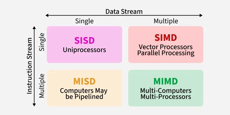
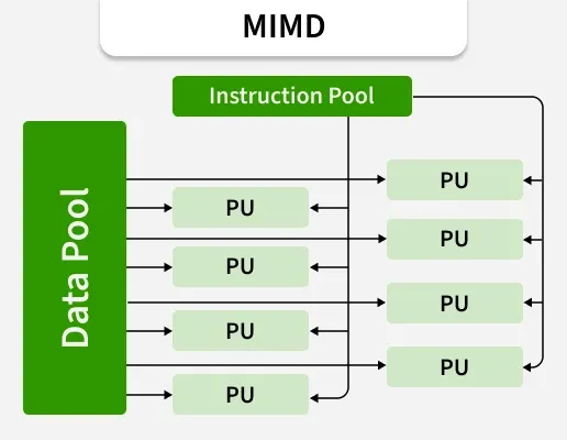
SISD, SIMD, MIMD, and SPMD are different ways to describe how a computer handles instructions and data during execution. The first three, SISD, SIMD, and MIMD, are part of Flynn's Taxonomy. This is a classification made by Michael Flynn based on how many instruction streams and data streams a system can process at the same time. SPMD is a bit different. It is a programming model, not a hardware type, and it is usually used on top of MIMD hardware.
SISD (Single Instruction, Single Data)
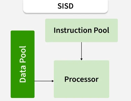
In SISD, there is only one instruction stream and one data stream at a time. This means the processor executes one instruction, on one piece of data, one after another. This is the normal model of a simple, traditional computer with a single processor. Most old personal computers and simple single-core CPUs work like this. Because there is no parallel work happening, performance can only be increased by things like pipelining or making the clock faster.
SIMD (Single Instruction, Multiple Data)
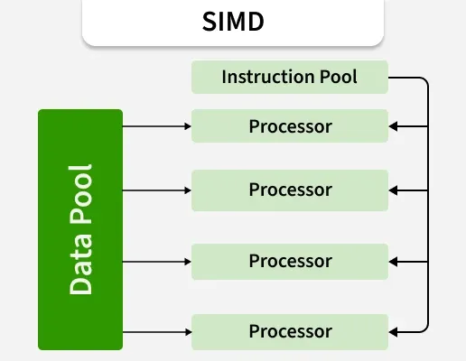
In SIMD, one single instruction is sent to many processing units at the same time, but each unit works on different data. So the same operation is done on many data values at once, in parallel. This is very useful for tasks like image processing, graphics, and scientific calculations where the same operation is repeated on large amounts of data. Examples of SIMD are array processors, vector processors, and modern GPUs. Also, many normal CPUs have SIMD instruction sets built in, like Intel's SSE and AVX.
MIMD (Multiple Instruction, Multiple Data)
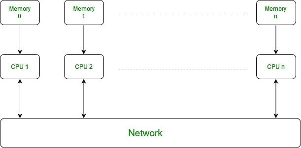
In MIMD, many processors run at the same time, but each one executes its own instruction stream on its own data. This is more flexible than SIMD because each processor can do a completely different task, or work on a different part of the same task, independently. Multicore processors, multiprocessor systems, and computer clusters are common examples of MIMD. MIMD systems can be divided into two types: shared-memory MIMD, where all processors use one common memory, and distributed-memory MIMD, where each processor has its own memory and they communicate through a network.
SPMD (Single Program, Multiple Data)
SPMD is not a hardware type like the other three. It is a programming model that usually runs on MIMD hardware. In SPMD, every processor runs the same program, but each one works on a different part of the data. Even though the program is the same, different processors can take different paths inside the program, for example using if-conditions based on the processor's ID. Since each processor runs on its own, without needing to stay in exact lockstep like SIMD, SPMD is more flexible. Because of this, SPMD is used a lot in real-world parallel programming, and it is the basic idea behind tools like MPI and CUDA programming for GPUs.
Comparison Table
| Model | Instruction Stream | Data Stream | Example |
|---|---|---|---|
| SISD | Single | Single | Simple, traditional CPU |
| SIMD | Single | Multiple | Vector processors, GPUs |
| MIMD | Multiple | Multiple | Multicore CPUs, clusters |
| SPMD | Multiple (same program) | Multiple | MPI programs, CUDA kernels |
SISD, SIMD, and MIMD describe how hardware handles instructions and data, starting from simple one-by-one execution to fully independent parallel execution. SPMD, on the other hand, describes a way of writing parallel programs, where the same program code runs on many processors but each processor works on different data. Together, these four ideas explain the basic types of parallelism used in modern computers, from a single-core processor to large parallel and distributed systems.
Q6. Differentiate between 80386, 80486 and Pentium processor.
Introduction
Intel 80386, 80486, and Pentium are three important processors in the history of x86 architecture, and each one represents a big step forward compared to the previous one. They came out one after another and each generation added new features, better performance, and more advanced design compared to the last.
Intel 80386
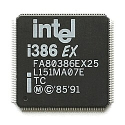
The 80386, also called i386, was released by Intel in 1985. It was the first 32-bit processor in the x86 family, while earlier processors like the 8086 and 80286 were only 16-bit. Because of this, the 80386 could handle 32-bit data and addresses, which means it could access much more memory, up to 4 GB, compared to earlier chips. It also introduced virtual memory support and protected mode, which allowed multitasking and better memory protection between different programs. But the 80386 did not have a built-in floating-point unit (FPU); it needed a separate chip called the 80387 math coprocessor if floating-point operations were needed. It also did not have any on-chip cache.
Intel 80486
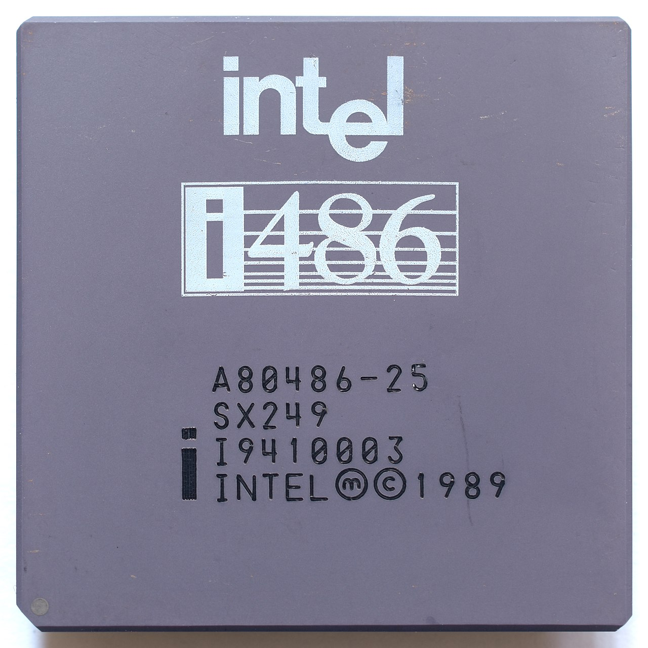
The 80486 came out in 1989 and was a big improvement over the 80386. The most important change is that the 80486 included a built-in floating-point unit right inside the chip, so a separate math coprocessor was no longer required for most versions. Another major addition was an on-chip cache memory (usually 8 KB), which reduced the need to access slower main memory again and again, and improved performance a lot. The 80486 also introduced pipelining into its execution, which allowed instructions to overlap during execution, something the 80386 did not have. Because of the pipeline and cache, the 80486 was much faster than the 80386 even at similar clock speeds.
Pentium
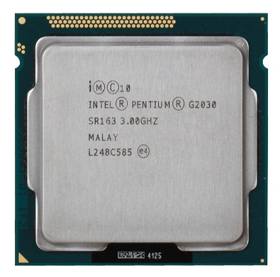
The Pentium processor was released in 1993 and represents another big jump. Unlike 80386 and 80486, which were part of Intel's numbered series (hence "486" instead of a name), Intel started using the name "Pentium" because numbers could not be trademarked. The Pentium introduced a superscalar architecture, meaning it had two execution pipelines (called u-pipe and v-pipe), so it could execute two instructions at the same time in one clock cycle, which was not possible in the 80486's single pipeline design. It also had a much improved floating-point unit, separate instruction and data caches, and introduced branch prediction to reduce pipeline stalls caused by branch instructions. The data bus was also widened to 64 bits, even though it was still internally a 32-bit processor, which allowed faster data transfer with memory.
Comparison Table
| Feature | 80386 | 80486 | Pentium |
|---|---|---|---|
| Year released | 1985 | 1989 | 1993 |
| Data width | 32-bit | 32-bit | 32-bit (64-bit data bus) |
| Floating-point unit | Separate (80387) | Built-in | Built-in, improved |
| On-chip cache | None | Yes (8 KB, unified) | Yes (separate for instruction and data) |
| Pipelining | No | Yes (single pipeline) | Yes (superscalar, dual pipeline) |
| Branch prediction | No | No | Yes |
| Instructions per cycle | 1 (multi-cycle) | About 1 (pipelined) | Up to 2 (superscalar) |
Overall, going from 80386 to 80486 to Pentium shows a clear pattern of improvement in Intel's processor design: the 80386 established 32-bit computing, the 80486 added pipelining, on-chip cache, and an integrated FPU, and the Pentium introduced superscalar execution with dual pipelines and branch prediction. Each generation reduced the number of clock cycles per instruction and increased the amount of work the processor could do at the same time, which is why the Pentium was much faster than the 80486, even beyond what higher clock speed alone would explain.
Q7. Explain different types of instruction format in MIPS.
Answer
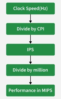
Million Instructions Per Second (MIPS):
MIPS measures the number of instructions a CPU can execute in one second, indicating its processing speed. A higher MIPS generally means the processor can handle more tasks, but it does not always reflect real-world performance.
- MIPS measures instruction throughput, not overall system speed.
- Higher MIPS doesn’t guarantee faster execution for complex programs.
- Actual performance depends on memory, cache, I/O, and instruction efficiency.
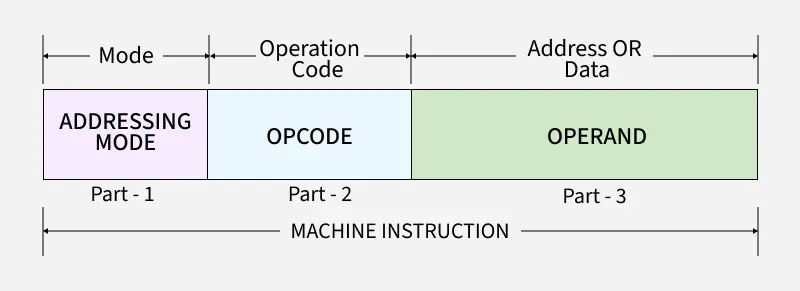
MIPS is a RISC architecture, so all its instructions have a fixed length of 32 bits. But even though every instruction is 32 bits, the way these 32 bits are divided depends on what kind of instruction it is.
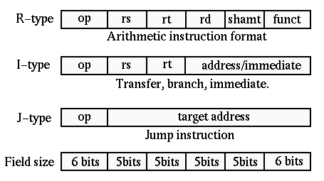
MIPS has three main instruction formats: R-type, I-type, and J-type. Each format arranges the bits in a different way, depending on how many registers or values the instruction needs to use. All MIPS instructions are encoded in binary.
All MIPS instructions are 32 bits long. Examples:
001000 10011010100000000000000100
000010 00000000000000000100000001
R-type (Register Type)
R-type format is used for instructions that work only with registers, like arithmetic and logic operations, for example add, sub, and, or, slt. This format has six fields:

Here, opcode is mostly 0 for R-type instructions, and the actual operation is decided by the funct field. rs and rt are the two source registers, rd is the destination register where the result is stored, and shamt is used only for shift instructions to say how many bits to shift.
R-type Example
Instruction: add $t0, $t1, $t2 (meaning $t0 = $t1 + $t2)
| opcode (6) | rs (5) | rt (5) | rd (5) | shamt (5) | funct (6) |
|   000000   |  01001  |  01010 |  01000 |   00000   |  100000   |
Here opcode is 000000, since it is an R-type instruction, rs = $t1 (register 9), rt = $t2 (register 10), rd = $t0 (register 8), shamt = 00000 because no shift is needed, and funct = 100000, which tells the ALU to perform addition.
Basic R-format Instructions
opcode(6 bits): Specifies the general operation class (always 000000 for R-type).rs(5 bits): First source register pointer.rt(5 bits): Second source register pointer.rd(5 bits): Destination register pointer where the result is saved.shamt(5 bits): Shift amount used for logical shift instructions (set to 0 for normal math).funct(6 bits): Function code which tells the ALU exactly which operation to perform (such as add or subtract).
Example
add $s0, $s1, $s2 (registers 16, 17, 18)

I-type (Immediate Type)
I-type format is used for instructions that need an immediate (constant) value, like load, store, branch, and arithmetic instructions with a constant, for example lw, sw, beq, addi. This format has four fields:
Field Breakdown:
opcode(6 bits): Specifies the unique operation type (such aslw,sw,beq, oraddi).rs(5 bits): Source register pointer or base register for load and store operations.rt(5 bits): Target register pointer acting as a destination for loads/addi, or as a source for stores.immediate/address(16 bits): Contains a 16-bit signed constant value or a memory address offset.
Here, rs is the source register (often used as a base address for load/store), rt is the destination register (or source, depending on instruction), and immediate is a 16-bit constant value, which can represent a number, an offset for memory address, or a branch offset.
I-type Example
Instruction: lw $t0, 4($s1) (meaning load word from memory address $s1 + 4 into $t0)
Here opcode = 100011 (the code for lw), rs = $s1 (register 17), which is the base register, rt = $t0 (register 8), which is where the loaded value goes, and immediate = 4, which is the offset added to $s1 to compute the memory address.
Another common I-type example is beq $t1, $t2, label, where rs and rt are the two registers being compared, and the immediate field holds the branch offset (in words) to jump to if $t1 equals $t2.
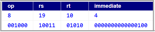
Example
add i $t2, $s3, 4 (registers 10 and 19)
J-type (Jump Type)
J-type format is used only for jump instructions, like j and jal, where the program needs to jump directly to a new address instead of computing it from registers. This format has two fields:
Here, the 26-bit address field gives a large part of the target address directly. Since MIPS instructions are word-aligned, this address is combined with the upper bits of the program counter and shifted to make the final full jump address.

J-type Example
Instruction: j 1024 (meaning jump directly to address 1024)
Here opcode = 000010 (the code for j), and the address field holds the target address (divided by 4, since instructions are word-aligned). The processor combines this 26-bit field with the top 4 bits of the current PC and shifts it left by 2 to get the final 32-bit jump address.
Field Breakdown:
opcode(6 bits): Specifies the jump operation type (such asjorjal).target address(26 bits): Holds the lower 26 bits of the target destination address.
Comparison Table
| Format | Used for | Fields |
|---|---|---|
| R-type | Register-register operations (add, sub, and, or) | opcode, rs, rt, rd, shamt, funct |
| I-type | Immediate operations, load/store, branch (addi, lw, sw, beq) | opcode, rs, rt, immediate |
| J-type | Jump instructions (j, jal) | opcode, address |
All three formats keep the same total length of 32 bits, which is one of the reasons MIPS is easy to fetch and decode in hardware. The opcode field is always the first 6 bits in every format, so the processor can quickly check what type of instruction it is before deciding how to read the rest of the bits. This fixed and simple structure is a key reason why MIPS is a good example of clean RISC design.
Q8. Explain the addressing modes of MIPS architecture.
Answer
Addressing mode means the method by which a processor finds the actual operand needed for an instruction. Different addressing modes give different ways to calculate the effective address of data. MIPS, being a RISC and load-store architecture, keeps its addressing modes very limited and simple, unlike CISC processors which support many complex addressing modes. MIPS mainly uses five addressing modes: register addressing, immediate addressing, base (displacement) addressing, PC-relative addressing, and pseudo-direct addressing.
Register Addressing
In register addressing, the operand value is directly present inside a register, and no memory access is needed at all. This is the fastest addressing mode because the ALU can read the operand directly from the register file.
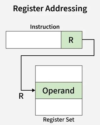
Example: add $t0, $t1, $t2
Here, the values of $t1 and $t2 are taken directly from registers, added together, and the result is stored in register $t0. No memory address calculation happens in this instruction, so this is a pure register addressing case.
Immediate Addressing
In immediate addressing, one of the operands is a constant value that is embedded directly inside the instruction itself, instead of being fetched from a register or memory.
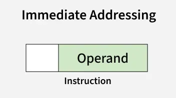
Example: addi $t0, $t1, 25
Here, 25 is the immediate value, taken directly from the 16-bit immediate field of the instruction, and added to the value in $t1. This mode is useful when the programmer needs to work with a known constant, and it avoids the extra step of loading that constant into a register first.
Base or Displacement Addressing
Base addressing, also called displacement addressing, is the primary addressing mode used for accessing memory in MIPS, specifically for load and store instructions. In this mode, the effective memory address is calculated by adding a constant offset (the displacement) to the value contained in a base register.
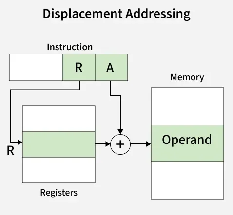
Example: lw $t0, 8($s1)
Here, $s1 is the base register, and 8 is the offset value. The effective address is computed as:
The processor then goes to that computed memory address, fetches the word stored there, and loads it into $t0. This mode is very important because MIPS follows a strict load-store philosophy, meaning ALU instructions never touch memory directly; only lw and sw type instructions are allowed to access memory, and both rely on this base addressing scheme.
PC-Relative Addressing
PC-relative addressing is used specifically in branch instructions, where the target address of the branch is calculated relative to the current value of the program counter (PC), instead of using an absolute address.
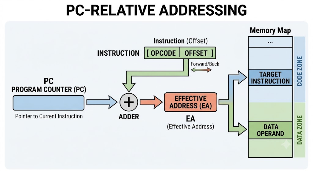
Example: beq $t1, $t2, label
Here, if the values in $t1 and $t2 are equal, the branch is taken, and the new PC is calculated as:
The immediate field holds a signed offset (in words, not bytes), which gets multiplied by 4 to convert it to a byte offset, and then added to PC + 4 (since MIPS already advances PC by 4 after fetching the current instruction). This mode allows branch targets to be reached efficiently without needing a full 32-bit absolute address embedded in the instruction.
Pseudo-Direct Addressing
Pseudo-direct addressing is used only in jump instructions like j and jal, where a large 26-bit address field from the instruction is combined with a few bits from the current PC to compute the actual jump target, since 26 bits alone are not enough to represent a full 32-bit address.
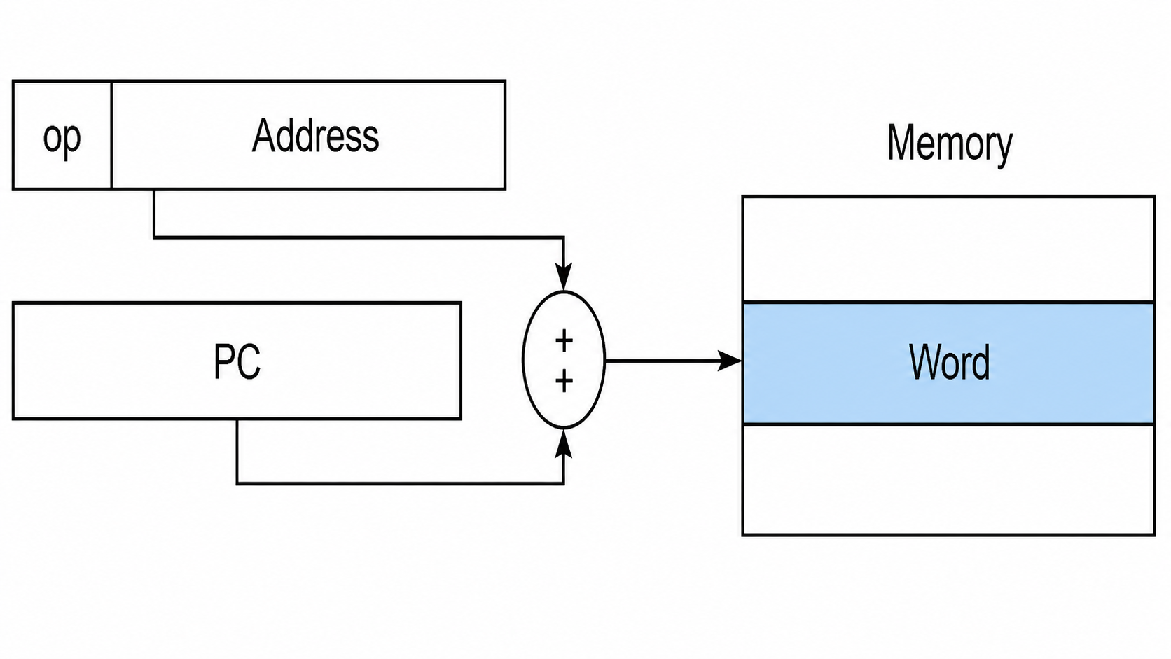
Example: j 4096
The effective jump address is computed as:
This means the top 4 bits are taken from the current PC (unchanged), the 26-bit address field from the instruction fills the next portion, and two zero bits are appended at the end because instructions are always word-aligned (multiples of 4 bytes). This is called "pseudo-direct" because it is not a fully direct address on its own; it still partially depends on the current PC value for its upper bits.
Comparison Table
| Addressing Mode | Operand Location | Example | Used In |
|---|---|---|---|
| Register | Inside register file | add $t0, $t1, $t2 |
R-type ALU instructions |
| Immediate | Embedded in instruction | addi $t0, $t1, 25 |
I-type constant operations |
| Base/Displacement | Memory[Register + Offset] | lw $t0, 8($s1) |
Load/store instructions |
| PC-relative | Memory[PC + 4 + offset×4] | beq $t1, $t2, label |
Conditional branches |
| Pseudo-direct | Memory[PC upper bits + address×4] | j 4096 |
Jump instructions |
MIPS keeps its addressing modes intentionally small in number compared to CISC processors, and this is one of the core reasons behind its simple hardware design and efficient pipelining. Each addressing mode is tied closely to a specific category of instruction, register addressing for ALU work, immediate addressing for constants, base addressing for load-store memory access, PC-relative for conditional branching, and pseudo-direct for unconditional jumps, which together cover all the addressing requirements of the architecture without adding unnecessary complexity.
Q9. Write down MIPS assembly code of f=(g+h)-(i+j), h=g+A[8].
To convert these high-level statements into MIPS assembly, first the variables need to be assigned to registers, since MIPS is a load-store architecture and all arithmetic operations happen only between registers, not directly between memory locations. Two separate expressions are given here, so each will be handled one at a time.
Register Assignment
Assume the variables are mapped to registers in the usual convention:
| Variable | Register |
|---|---|
| f | $s0 |
| g | $s1 |
| h | $s2 |
| i | $s3 |
| j | $s4 |
Also assume the base address of array A is already stored in register $s6.
Part 1: f = (g+h) - (i+j)
This expression has two separate additions first, and then a subtraction between the two results. Since MIPS instructions can only take two source operands and produce one result at a time, this needs to be broken down into three simple steps using temporary registers.
add $t0, $s1, $s2      # $t0 = g + h
add $t1, $s3, $s4      # $t1 = i + j
sub $s0, $t0, $t1      # f = $t0 - $t1 = (g+h) - (i+j)
Here, first the sum of g and h is computed and stored in temporary register $t0, then the sum of i and j is computed and stored in $t1, and finally the subtraction between these two temporary results is done, with the final answer placed into $s0, which represents f.
Part 2: h = g + A[8]
This statement needs an array access. Since A[8] means the element at index 8 of array A, and MIPS memory is byte-addressed while each word takes 4 bytes, the actual byte offset for A[8] from the base address is calculated as:
So the instruction to load A[8] uses base addressing mode with an offset of 32 from the base register $s6.
Here, first the value of A[8] is loaded from memory into temporary register $t0 using base addressing, with $s6 as the base and 32 as the byte offset. Then this loaded value is added to g (stored in $s1), and the result is placed into $s2, which represents h.
Q10. Explain the assembly code of if (i==j) f = g+h; else f = g-h;
Answer:
This is a conditional statement, and MIPS does not have a direct "if-else" instruction like high-level languages. Instead, conditional behavior is implemented using branch instructions along with labels, which control the flow of execution based on whether a condition is true or false. The general strategy is to test the condition, and if it fails, jump over the "if" part directly to the "else" part, using unconditional and conditional jumps together.
Register Assignment
| Variable | Register |
|---|---|
| f | $s0 |
| g | $s1 |
| h | $s2 |
| i | $s3 |
| j | $s4 |
Logic Behind the Code
In high-level thinking, the condition is if (i==j). But in MIPS, it is usually easier to code the opposite (negated) condition first, and branch away if that condition is true, meaning: "if i is NOT equal to j, skip the if-part and go directly to the else-part." This is a very common and standard trick used while converting if-else into assembly.
Assembly Code
        bne  $s3, $s4, Else     # if (i != j) goto Else
        add  $s0, $s1, $s2      # f = g + h   (this runs only if i == j)
        j    Exit                # skip the else part

Else:   sub  $s0, $s1, $s2      # f = g - h   (this runs only if i != j)

Exit:
Line by Line Explanation
The first instruction, bne $s3, $s4, Else, checks whether i and j are not equal. If they are indeed not equal, the branch is taken, and control jumps directly to the label Else, skipping the "if" part entirely. If i and j are equal, the branch is not taken, and execution simply continues to the next line.
The second instruction, add $s0, $s1, $s2, computes f = g + h, and this line only executes when the branch above was not taken, meaning i was equal to j, which correctly matches the original if-condition.
The third instruction, j Exit, is an unconditional jump that is necessary right after the if-part. Without this jump, execution would simply fall through into the else-part below and wrongly execute the subtraction as well. So this jump ensures that once the if-part is done, the program skips over the else-part completely.
At the label Else:, the instruction sub $s0, $s1, $s2 computes f = g - h, and this only runs when control jumped here directly from the bne instruction, meaning i was not equal to j.
Finally, the label Exit: marks the point where both paths, if and else, converge back together, and the program continues normally after the conditional block.
Control Flow Summary
This example shows the standard pattern used in MIPS for converting any if-else structure: negate the original condition, branch to the else-label if the negated condition is true, place an unconditional jump at the end of the if-block to skip the else-block, and finally use a common exit label where both branches join back together. This same pattern, negate-and-branch plus jump-and-label, is the foundation for implementing all kinds of conditional and loop structures in MIPS assembly.
Q 11. What is a Basic Block? Explain with Example.
Answer:
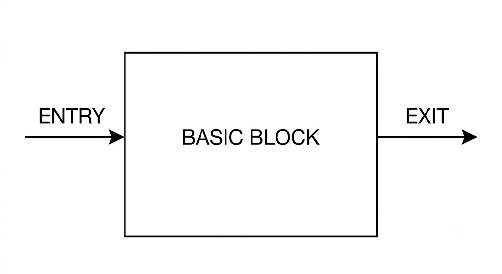
A basic block is a fundamental concept used in compiler design and program analysis, especially while doing optimization or building a control flow graph. It is a sequence of instructions inside a program that has one clear entry point and one clear exit point, meaning execution always starts from the first instruction of the block and always ends at the last instruction, without any possibility of jumping in the middle or jumping out in the middle.
Definition
A basic block is defined as a straight-line sequence of code with the following two properties: first, there is no branch or jump target anywhere inside the block except at the very first instruction, meaning nothing from outside can jump into the middle of the block; second, there is no branch, jump, or control transfer instruction anywhere inside the block except possibly at the very last instruction, meaning control cannot leave the block from the middle either. In simple words, once execution enters a basic block, it will always execute every single instruction inside it, one after another, in order, without any interruption, until it reaches the end.
Why Basic Blocks Are Important
Basic blocks are important because compilers use them to build something called a control flow graph (CFG), where each basic block becomes a single node, and edges between nodes represent possible jumps or branches between blocks. This is very useful for optimization techniques, such as detecting dead code, register allocation, and instruction scheduling, since the compiler can safely assume that everything inside one basic block always executes together as one unit.
Example
Consider this simple piece of MIPS-like code:
1:  add  $t0, $s1, $s2
2:  sub  $t1, $s3, $s4
3:  bne  $t0, $t1, Label1
4:  add  $s0, $t0, $t1
5:  j    Exit
Label1:
6:  sub  $s0, $t0, $t1
Exit:
7:  sw   $s0, 0($s5)
If this code is broken into basic blocks, it looks like this:
Block A (lines 1–3): starts at line 1, since that's the beginning of the program, and ends at line 3, because line 3 has a branch instruction (bne), which can transfer control elsewhere. Nothing inside lines 1 to 3 is a jump target, so this whole group stays together as one block.
Block B (lines 4–5): starts at line 4, because line 3's branch could either fall through here or jump to Label1, making line 4 a possible entry point. It ends at line 5, because line 5 has an unconditional jump (j Exit).
Block C (line 6): starts at line 6, because Label1 is a branch target, meaning some other instruction can jump directly here, and this makes it a new entry point. It ends at line 6 itself, since there's only one instruction before falling through to the next label.
Block D (line 7): starts at line 7, because Exit is a target for both the jump in line 5 and the fall-through from block C, and this line is the final instruction of the program.
Visual Representation
This shows that after Block A, execution can go either to Block B (if the branch is not taken) or to Block C (if the branch is taken), and both paths eventually join at Block D.
A basic block is essentially the smallest safe unit of code that a compiler can treat as a single, uninterrupted piece, since it always starts execution from the top and always finishes at the bottom without any branching happening inside. Identifying basic blocks correctly is the first and most essential step before building a control flow graph, and it forms the base for almost all compiler optimization techniques used later in the compilation process.
Q12. Explain the steps of compilation process of a C program.
Answer:
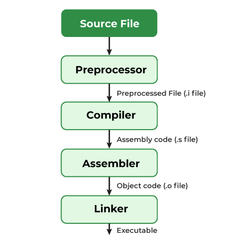
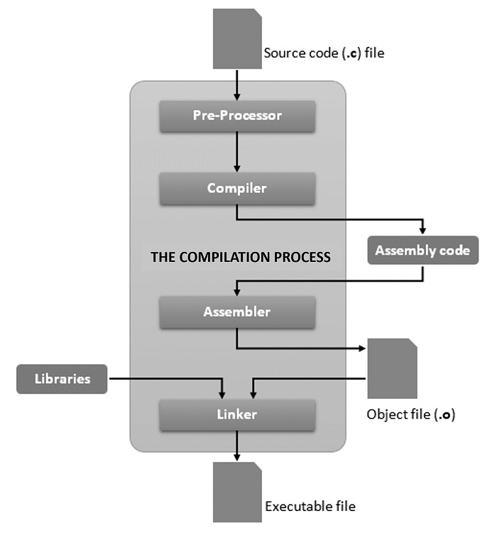
Compilation is basically the process of converting a C source program, which is written in a human-readable high-level language, into an executable machine code file that the processor can run directly. This is not a single-step process, rather it goes through four different stages, and each stage does one specific job and then passes its output to the next stage.
The four main stages are:
- Preprocessing
- Compilation (source to assembly)
- Assembly (assembly to machine code)
- Linking
The C program goes through the following phases during compilation:
Preprocessing
This stage is handled by a program called the preprocessor. In this stage, all the lines starting with #, such as #include, #define, and #ifdef, are processed and expanded properly.
- It removes all the comments in the source file(s).
- It includes the code of the header file(s), which is a file with extension .h which contains C function declarations and macro definitions.
- It replaces all of the macros (fragments of code which have been given a name) by their values.
The output of this step will be stored in a file with a ".i" extension, so here it will be in "main.i".
In order to stop the compilation right after this step, we can use the option "-E" with the gcc command on the source file, and press Enter.
#include <stdio.h>gets replaced by the actual content present inside the stdio.h header file- Any macro defined using
#definegets substituted wherever it is being used inside the code - Comments get removed completely
Output of this stage is still a C file only, usually having extension .i, but now it is fully expanded, having no preprocessor directives left.
Compilation (Source to Assembly)
The compiler generates the IR code (Intermediate Representation) from the preprocessed file, so this will produce a ".s" file. That being said, other compilers might produce assembly code at this step of compilation.
We can stop after this step with the "-S" option on the gcc command, and press Enter.
This is what the main.s file should look like −
.file   "helloworld.c"
   .text
   .def __main; .scl    2;  .type   32; .endef
   .section .rdata,"dr"
.LC0:
   .ascii "Hello, World! \0"
   .text
   .globl   main
   .def main;   .scl    2;  .type   32; .endef
   .seh_proc    main
main:
   pushq    %rbp
   .seh_pushreg %rbp
   movq %rsp, %rbp
   .seh_setframe    %rbp, 0
   subq $32, %rsp
   .seh_stackalloc  32
   .seh_endprologue
   call __main
   leaq .LC0(%rip), %rcx
   call puts
   movl $0, %eax
   addq $32, %rsp
   popq %rbp
   ret
   .seh_endproc
   .ident   "GCC: (x86_64-posix-seh-rev0, Built by MinGW-W64 project) 8.1.0"
   .def puts;   .scl    2;  .type   32; .endef
Assembly (Assembly to Machine Code)
This stage is handled by a program called the assembler. The assembler takes the human-readable assembly instructions, like add $t0, $t1, $t2, which were generated in previous stage, and converts them into actual binary machine code, strictly following the instruction format of that target architecture, for example R-type or I-type format in case of MIPS.
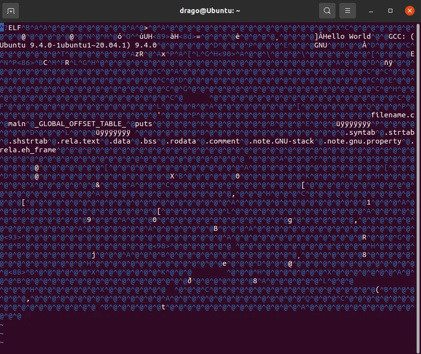
Output of this stage is called an object file, usually having extension .o or .obj. This object file already contains machine code, but it is still not directly executable, because it may have references to some external functions or variables which are defined somewhere else, like inside a library file.
Linking
This is the last stage, handled by a program called the linker. Since a C program mostly uses functions coming from external libraries, like printf from stdio.h, and it may also be written across multiple different source files, the job of linker is to:
- Combine all the required object files together
- Resolve all external references properly by matching each function call to its actual definition
- Link in the necessary library code wherever needed
Final output of this stage is a single executable file, which contains complete machine code, and is now ready to be loaded into memory and run directly by the operating system.
Complete Flow
| Stage | Tool Used | Input | Output |
|---|---|---|---|
| Preprocessing | Preprocessor | .c file |
Expanded .i file |
| Compilation | Compiler | .i file |
Assembly .s file |
| Assembly | Assembler | .s file |
Object .o file |
| Linking | Linker | .o file(s) + libraries |
Executable file |
Each of these four stages, that is preprocessing, compilation, assembly, and linking, brings the program one step nearer to its actual machine-executable form, starting from human-readable C code all the way down to raw binary instructions which the hardware can understand directly. Understanding this full pipeline is quite important also, because it clearly shows where different types of errors can occur, for example syntax errors get caught during compilation stage itself, while undefined function errors get caught only during linking stage, and it also explains why even one small change in source code needs to pass through this entire chain again before it can actually run on the machine.
Q13. How the performance of a microprocessor is measured? Explain with example.
Answer:
Performance of a microprocessor basically means how fast it can execute a given program or a given task. It is not enough to just look at clock speed of a processor, because actual performance depends on several other factors also, like number of instructions, cycles taken per instruction, and clock cycle time. So performance is generally measured using a proper formula, and not just by comparing GHz values directly.
Basic Performance Equation
The most fundamental equation used for measuring processor performance is the CPU time equation, and it can be written as:
Here, each term has its own meaning:
- Instruction Count (IC) means total number of instructions executed for a particular program
- CPI (Cycles Per Instruction) means average number of clock cycles needed to execute one instruction
- Clock Cycle Time means time taken for one single clock cycle, which is basically the inverse of clock frequency
This same equation can also be written using clock frequency directly, instead of clock cycle time:
So basically, lower CPU time means better performance, meaning the processor is finishing the same task in less time.
Other Important Performance Metrics
Along with CPU time, there are some other common metrics also used for measuring performance:
- MIPS (Million Instructions Per Second) shows how many million instructions the processor executes in one second
- Clock Frequency shows how many clock cycles happen in one second, measured in Hz, and higher frequency generally means faster processing, but only if CPI stays same
- CPI itself is also used separately as a performance indicator, since lower CPI means processor is completing instructions in fewer cycles on average
Example
Suppose a program has:
- Instruction Count = 50 million instructions
- Average CPI = 2
- Clock Frequency = 1 GHz (which means clock cycle time = 1 ns)
Then CPU time can be calculated as:
So this processor is taking 0.1 seconds to finish this particular program.
Now suppose another processor B runs the same program with:
- Instruction Count = 50 million (same program, same instructions)
- Average CPI = 1.5
- Clock Frequency = 800 MHz (clock cycle time = 1.25 ns)
Then CPU time for processor B becomes:
So even though processor B has lower clock frequency compared to processor A, it is still faster in actual execution time, because its CPI is quite lower. This example shows clearly why clock speed alone cannot decide performance, and CPI plays a very important role too.
Comparison Table
| Processor | Instruction Count | CPI | Clock Frequency | CPU Time |
|---|---|---|---|---|
| A | 50 million | 2.0 | 1 GHz | 0.1 s |
| B | 50 million | 1.5 | 800 MHz | 0.09375 s |
Specialized Operations & Hardware Factors
- MIPS (Million Instructions Per Second): A legacy unit for measuring general instruction throughput.
- FLOPS (Floating Point Operations Per Second): Used to measure performance in intensive scientific and engineering calculations.
- Multi-Core & Architecture: Multi-core processors allow for parallel processing, dramatically multiplying a chip's capabilities without necessarily raising the clock speed.
So performance of a microprocessor cannot be judged only by looking at clock frequency, rather it depends on combination of three factors together, that is instruction count, CPI, and clock cycle time. A processor with higher clock speed can still be slower overall if its CPI is high, exactly like shown in above example. This is why CPU time equation is considered the most reliable and standard way for comparing performance between different processors, instead of just comparing raw GHz numbers.
Q14. What do you mean by IPC and CPI?
Answer:
IPC and CPI are two related terms used for measuring how efficiently a processor executes instructions. Both terms basically talk about the relationship between number of instructions and number of clock cycles, but they look at this relationship from opposite directions. Understanding these two terms properly is important, because they directly connect to the performance equation discussed in previous answer.
CPI (Cycles Per Instruction)
CPI means average number of clock cycles that are needed to execute one single instruction. It is calculated as:
If a processor takes more clock cycles on average to complete each instruction, then its CPI value will be high, which generally means the processor is less efficient. Different types of instructions can also have different CPI values, for example a simple add instruction might take only 1 cycle, but a multiply or divide instruction might take several cycles, so the overall CPI of a program is basically a weighted average across all instruction types used in that program.
IPC (Instructions Per Cycle)
IPC means average number of instructions that a processor is able to complete in one single clock cycle. It is basically the inverse of CPI, and is calculated as:
If a processor is able to complete more than one instruction in a single cycle, like in superscalar processors, then its IPC value goes above 1, and this generally means the processor is more efficient and doing more parallel work.
Relationship Between IPC and CPI
Since IPC and CPI are just inverse of each other, higher IPC always means lower CPI, and lower IPC always means higher CPI. So basically:
A processor designer generally wants CPI to be as low as possible, or in other words, wants IPC to be as high as possible, because this directly means better performance, since fewer cycles are being wasted per instruction.
Example
Suppose a program has:
- Total Instruction Count = 10 million
- Total Clock Cycles taken = 20 million
Then CPI can be calculated as:
And IPC can be calculated as:
This means, on average, this processor is taking 2 clock cycles to complete one instruction, or in other words, completing only half an instruction per clock cycle.
Now suppose a superscalar processor B runs the same program with:
- Total Instruction Count = 10 million (same program)
- Total Clock Cycles taken = 6 million
Then:
This shows processor B is completing more than 1 instruction per cycle on average, which is only possible because of superscalar design, where multiple instructions get issued and executed in parallel within same clock cycle.
Comparison Table
| Processor | Instruction Count | Clock Cycles | CPI | IPC |
|---|---|---|---|---|
| A | 10 million | 20 million | 2.0 | 0.5 |
| B | 10 million | 6 million | 0.6 | 1.67 |
CPI and IPC are basically two sides of the same coin, one measuring cycles needed per instruction, and other measuring instructions completed per cycle. Lower CPI or higher IPC both indicate better processor efficiency, and this is exactly why modern superscalar and pipelined processors are designed with the goal of pushing IPC as high as possible, since that directly improves overall performance as per the CPU time equation discussed earlier.
**Q15. Suppose machine A has a clock tick of 1 ns (1e-9 sec) and a CPI of 2.0 for a program P. Suppose machine B has the same ISA as machine A, but has a clock tick of 2 ns and a CPI of 1.2 for program P. Which machine is “faster”? **
Answer:
Given data in the problem:
- Clock tick of Machine A (\(T_A\)) = \(1\text{ ns}\)
- CPI of Machine A (\(\text{CPI}_A\)) = \(2.0\)
- Clock tick of Machine B (\(T_B\)) = \(2\text{ ns}\)
- CPI of Machine B (\(\text{CPI}_B\)) = \(1.2\)
Both machines are using the same Instruction Set Architecture (ISA) for running the same program P. Therefore, the total number of instructions will be exactly equal for both machines. Let us assume this common Instruction Count is \(I\).
We know the standard university formula for calculating the CPU performance time:
Calculation for Machine A
By putting the values of Machine A in the formula:
=> \(\text{CPU Time}_A = I \times \text{CPI}_A \times T_A\)
=> \(\text{CPU Time}_A = I \times 2.0 \times 1\text{ ns}\)
=> \(\text{CPU Time}_A = 2.0 \times I\text{ ns}\)
Calculation for Machine B
By putting the values of Machine B in the formula:
=> \(\text{CPU Time}_B = I \times \text{CPI}_B \times T_B\)
=> \(\text{CPU Time}_B = I \times 1.2 \times 2\text{ ns}\)
=> \(\text{CPU Time}_B = 2.4 \times I\text{ ns}\)
Comparison and Conclusion
Now we will compare the total execution time of both machines to find which machine is faster:
=> \(\text{CPU Time}_A = 2.0 \times I\text{ ns}\)
=> \(\text{CPU Time}_B = 2.4 \times I\text{ ns}\)
=> \(2.0 \times I < 2.4 \times I\)
=> \(\text{CPU Time}_A < \text{CPU Time}_B\)
Machine A takes less execution time than Machine B to complete the program P. Therefore, Machine A is faster.
Q16: Suppose 2GHz machine A executes 200e6 instructions in 6 s for a program P. Suppose 3GHz machine B executes 160e6 instructions in 3 s for the same program P. Which machine is “faster,” and by how much? How many instructions per second (MIPS) are executed by each machine? What is the CPI for each machine? If a second program Q has the same CPI as P and takes 3 s on machine A and 4 s on machine B, what is the IC of Q on each machine?
Answer:
Given Data for Program P
- Clock Rate of Machine A = \(2\text{ GHz} = 2 \times 10^9\text{ Hz}\)
- Execution Time on Machine A (\(\text{Time}_A\)) = \(6\text{ seconds}\)
- Instruction Count for Machine A (\(\text{IC}_A\)) = \(200 \times 10^6\) instructions
- Clock Rate of Machine B = \(3\text{ GHz} = 3 \times 10^9\text{ Hz}\)
- Execution Time on Machine B (\(\text{Time}_B\)) = \(3\text{ seconds}\)
- Instruction Count for Machine B (\(\text{IC}_B\)) = \(160 \times 10^6\) instructions
Part 1: Finding Which Machine is Faster and By How Much
To find which machine is faster, we just look at the total execution time taken for the same program P.
- \(\text{Time}_A = 6\text{ seconds}\)
- \(\text{Time}_B = 3\text{ seconds}\)
Since Machine B takes less time, Machine B is faster.
Now, we will calculate how much faster Machine B is by taking the performance ratio:
=> \(\text{Performance Ratio} = \frac{6}{3}\)
=> \(\text{Performance Ratio} = 2\)
So, Machine B is exactly 2 times faster than Machine A.
Part 2: Calculating MIPS (Millions of Instructions Per Second) for Each Machine
The formula to calculate MIPS is written below:
Calculation for Machine A:
=> \(\text{MIPS}_A = \frac{200 \times 10^6}{6 \times 10^6}\)
=> \(\text{MIPS}_A = \frac{200}{6}\)
=> \(\text{MIPS}_A = 33.33\)
Calculation for Machine B:
=> \(\text{MIPS}_B = \frac{160 \times 10^6}{3 \times 10^6}\)
=> \(\text{MIPS}_B = \frac{160}{3}\)
=> \(\text{MIPS}_B = 53.33\)
Part 3: Calculating CPI (Cycles Per Instruction) for Each Machine
We know the standard CPU time formula:
By rearranging this formula, we get the expression for CPI:
Calculation for Machine A:
=> \(\text{CPI}_A = \frac{6 \times (2 \times 10^9)}{200 \times 10^6}\)
=> \(\text{CPI}_A = \frac{12 \times 10^9}{200 \times 10^6}\)
=> \(\text{CPI}_A = \frac{12000 \times 10^6}{200 \times 10^6}\)
=> \(\text{CPI}_A = \frac{12000}{200}\)
=> \(\text{CPI}_A = 60\)
Calculation for Machine B:
=> \(\text{CPI}_B = \frac{3 \times (3 \times 10^9)}{160 \times 10^6}\)
=> \(\text{CPI}_B = \frac{9 \times 10^9}{160 \times 10^6}\)
=> \(\text{CPI}_B = \frac{9000 \times 10^6}{160 \times 10^6}\)
=> \(\text{CPI}_B = \frac{9000}{160}\)
=> \(\text{CPI}_B = 56.25\)
Part 4: Calculating Instruction Count (IC) for Program Q
Given conditions for second program Q:
- CPI of program Q is same as program P for both machines (\(\text{CPI}_A = 60\), \(\text{CPI}_B = 56.25\)).
- Execution time of Q on Machine A (\(\text{Time}_{A(Q)}\)) = \(3\text{ seconds}\)
- Execution time of Q on Machine B (\(\text{Time}_{B(Q)}\)) = \(4\text{ seconds}\)
We will use the modified formula to calculate Instruction Count:
$\(\text{IC} = \frac{\text{Execution Time} \times \text{Clock Rate}}{\text{CPI}}\)$
Instruction Count of Q on Machine A:
=> \(\text{IC}_{A(Q)} = \frac{3 \times (2 \times 10^9)}{60}\)
=> \(\text{IC}_{A(Q)} = \frac{6 \times 10^9}{60}\)
=> \(\text{IC}_{A(Q)} = 100 \times 10^6\) instructions
Instruction Count of Q on Machine B:
=> \(\text{IC}_{B(Q)} = \frac{4 \times (3 \times 10^9)}{56.25}\)
=> \(\text{IC}_{B(Q)} = \frac{12 \times 10^9}{56.25}\)
=> \(\text{IC}_{B(Q)} = 213.33 \times 10^6\) instructions
Q17. Explain the multiplication algorithm with an example.
Answer:
Multiplication in a processor cannot be done directly using one single ADD instruction like normal addition, because multiplication is basically a repeated process, and hardware needs a proper systematic algorithm to perform it using limited resources, like registers, an adder, and shifting logic. Booth's algorithm is one of the most important methods used for this purpose, and its main advantage is that it treats signed numbers in a uniform manner, without needing separate preprocessing steps for negative numbers.
Core Registers Used in Hardware Architecture
- Multiplicand Register (M): This register holds the multiplicand value, and it stays fixed throughout the whole process.
- Multiplier Register (Q): This register stores the binary multiplier value that needs to be multiplied, and its LSB is checked at every step, then it keeps shifting right.
- Extra Bit Q(-1): This is an additional flip-flop placed right after the LSB of Q, initialized to fictitious zero, and it is used along with Q(0) to detect the boundary of consecutive ones in the multiplier.
- Accumulator Register (A): This is initialized to zero at the beginning, and it holds the shifting partial results (the running sum or difference) during execution.
- Sequence Counter (Size): It keeps track of the number of bits remaining to be processed, and it decreases by 1 after every iteration, until it reaches 0 and the loop ends.
Hardware Modifications Needed
Two modifications are needed to the basic multiplication hardware, in order to implement Booth's algorithm properly:
- Q register size is extended from 4 to 5 bits, so that the extra position will initially hold the fictitious zero, that is \(Q(-1)\)
- The 4-bit parallel adder is replaced with a 4-bit adder/subtractor, since Booth's algorithm needs both addition and subtraction
Flowchart of the Algorithm
The accompanying flowchart specifies the mechanics of a \(4 \times 4\) two's complement sequential Booth's multiplier. First, registers are initialized as \(A = 0\), \(M = multiplicand\), \(Q = multiplier\), \(Q(-1) = 0\), and \(Size = 4\).
Then the loop starts, where two bit pairs are checked:
- If \(Q(0) = 0\) and \(Q(-1) = 1\), then \(A = A + M\)
- If \(Q(0) = 1\) and \(Q(-1) = 0\), then \(A = A - M\)
- If \(Q(0)\) and \(Q(-1)\) are same, no operation happens
After this step, arithmetic shift right is done on combined AQ register, then \(Size = Size - 1\), and the loop repeats until \(Size = 0\), at which point the process ends.
Booth's Recording Table
Booth's algorithm works by inspecting two bits at a time, that is current multiplier bit \(q_i\) and previous bit \(q_{i-1}\), and deciding the implied action based on this pair, following this recording table:
| Multiplier Bits Inspected \(q_i q_{i-1}\) | Recorded Digit Underneath Position \(j\) | Implied Action in Position \(j\) |
|---|---|---|
| 0 0 | 0 | None |
| 0 1 | 1 | Add M |
| 1 0 | \(\bar{1}\) | Sub M |
| 1 1 | 0 | None |
Example Trace
To see how this procedure works, the following trace is provided. Assume that \(M = -4 = 1100\) and \(Q = 7 = 0111\).
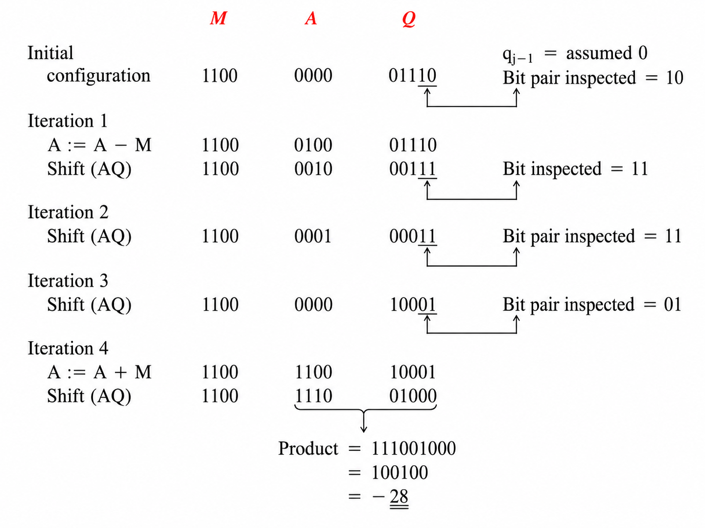
Observations from the Trace
- Preprocessing steps are unnecessary, so Booth's algorithm treats signed numbers in a uniform manner
- Only one addition and one subtraction are needed to carry out this multiplication (observe that \(M * 7 = M * (8-1) = (8M - M)\))
- Booth's algorithm is called a skipping over 1 technique, since it skips over a block of consecutive ones, and this process resembles the differentiation process
This flowchart and trace together show exactly how Booth's algorithm handles a signed multiplication like \(-4 \times 7\), producing the correct result of \(-28\), using only shifting, and one addition and one subtraction, instead of repeated additions for every single bit. This skip-over-1s behavior is precisely what makes Booth's algorithm more efficient compared to the plain shift-and-add method, especially when the multiplier has long runs of consecutive ones.
Q18. Explain the division algorithm with example.
Answer:
Given a dividend (D) and a divisor (V), the quotient (Q) and remainder (R) are related as follows:
A Q that will make the product VQ very close to D is needed, and this implies that the remainder R of a division will always be in the range \(0 \leq R < V\). When examining the relation \(D \approx Q \times V\), a great deal of similarity between multiplication and division can be recognized. The following are analogous pairs: the product and the dividend, the quotient and the multiplicand, and the multiplier and the divisor. Such a relationship implies that the same hardware unit used for multiplication can be used to perform division, after some modification. In a sequential multiplier, the product is obtained by adding shifted multiplicands, however, in case of division, the quotient is obtained by repeatedly subtracting the shifted divisor from the dividend.
Paper and Pencil Division Technique
Subtractive division algorithms are derived from the paper and pencil approach, using \(D = 22\) and \(Q = 3\) as illustration.
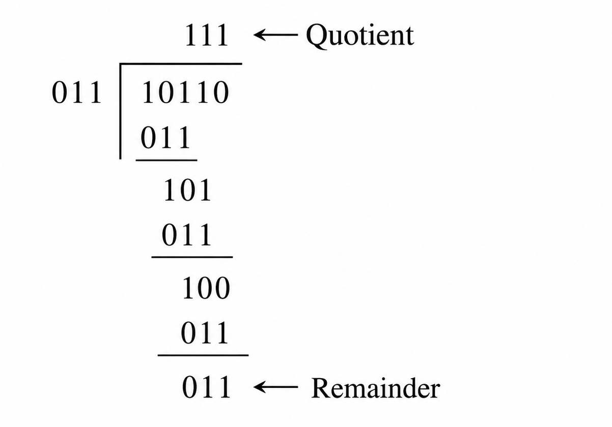
In this method, one quotient bit per iteration is generated. First, the divisor is lined up against the dividend, and subtraction from dividend is tried. If result of subtraction is positive, a 1 is entered for the quotient, and divisor is shifted one position to the right, then the whole process is repeated. However, if divisor cannot be subtracted from dividend without yielding a negative result, a 0 is entered for the quotient, and divisor is shifted to the right without subtracting. This process continues until all bits of dividend are covered.
Restoring Division Algorithm
This algorithm can be mechanized with the following modifications:
- Instead of moving the divisor, the dividend is shifted to the left. Three 4-bit registers, M, A, and Q, are used when dividing two 4-bit numbers. Register M holds the divisor. Registers A and Q are initialized with the dividend, where A is cleared to 0, and Q holds the dividend.
- In each iteration, contents of A and Q are shifted left first, then contents of M are subtracted from A. If result of subtraction is positive, a 1 is placed into the vacant position created by left shift; otherwise a 0 is placed there.
- This process is repeated until all bits of the dividend, originally stored in Q, are moved into A. When the algorithm terminates, A register contains the remainder, and Q register contains the quotient.
- When result of subtraction yields a negative answer, contents of A must be restored, by adding contents of A register with M, before beginning next iteration. This step is why the algorithm is called a restoring division algorithm.
The basic steps of this algorithm are:
- Step 1: Shift A and Q registers to the left.
- Step 2: Subtract M from A.
- Step 3: If result of subtraction is positive, set Q[0] = 1; otherwise set Q[0] = 0.
To divide two n-bit numbers using restoring division algorithm, these steps are repeated n times.
Restoring Division Example
Assume \(M = 3 = 00011\) and dividend is such that \(Q = 1011\).
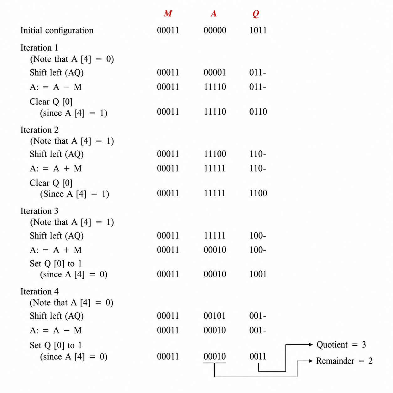
From this trace, Quotient = 3 and Remainder = 2.
The restoring division algorithm needs n subtractions, and extra additions when dividing two n-bit numbers, due to the restoration process. Exact number of extra additions depends on data, so it cannot be figured in deterministic manner. Assuming, however, that 50% of subtraction operations yield a negative result, then n/2 extra additions are needed.
Nonrestoring Division Algorithm
By properly restructuring the restoring division algorithm, the need for a restoration step can be eliminated, and this is known as the nonrestoring division algorithm.
Assuming that Step 3 is performed first, then Step 1 is followed by Step 2, and computation starts immediately after subtraction, one of the following must be performed:
- If sign of number stored in A register is positive, shift A and Q registers left, and subtract contents of M register from A register. Note that shifting A register left is identical to computing 2A, so a left shift followed by subtraction can be merged into one operation:
- If sign of number stored in A register is negative, first restore A by adding contents of A register with M register, then shift A and Q registers left. As a result of these three operations combined into one, the following is computed:
The least significant bit of Q register must be set or cleared depending on result in A register. Q[0] is set to 1 if sign bit of A register is zero, otherwise Q[0] is reset to 0.
This algorithm eliminates the need to restore contents of A within the main loop, and this technique may need one restoration step only at the end, to restore the final remainder.
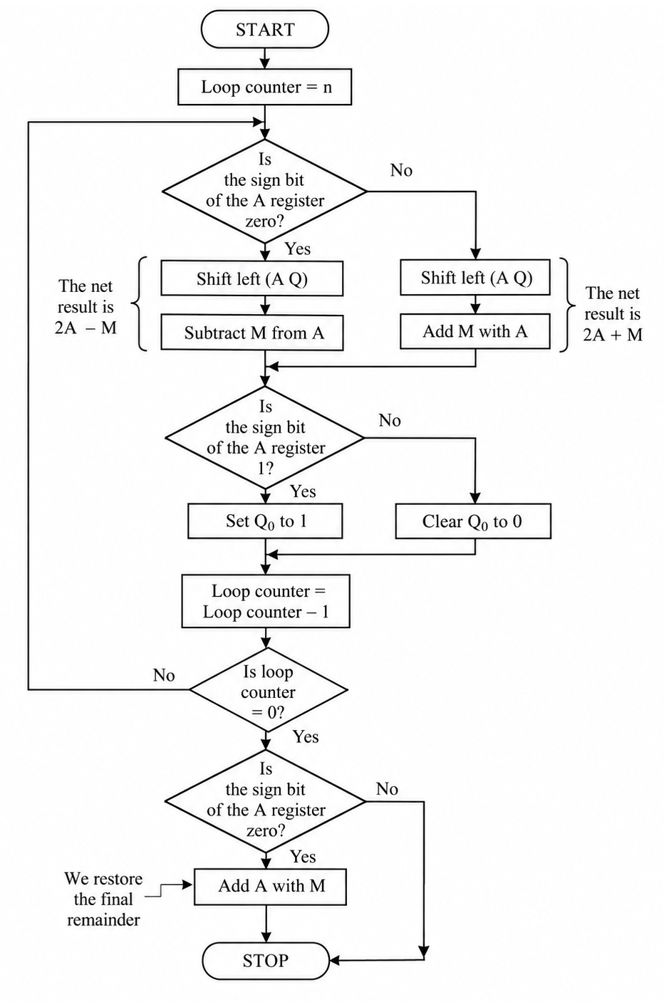
Nonrestoring Division Flowchart
The flowchart works as follows: loop counter is initialized to n. Then sign bit of A register is checked. If sign bit is zero, AQ is shifted left and M is subtracted from A (net result \(2A - M\)). If sign bit is not zero, AQ is shifted left and M is added with A (net result \(2A + M\)). After this, sign bit of A register is checked again: if it is 1, Q₀ is set to 1; if not, Q₀ is cleared to 0. Loop counter is then decremented by 1, and checked against 0. If loop counter is not 0, the process repeats. If loop counter is 0, sign bit of A is checked one final time: if it is not zero, A is restored by adding M with A, to recover the final remainder, and the process stops.
Nonrestoring Division Example
Assume \(M = 3 = 00011\) and \(Q = 1011\).
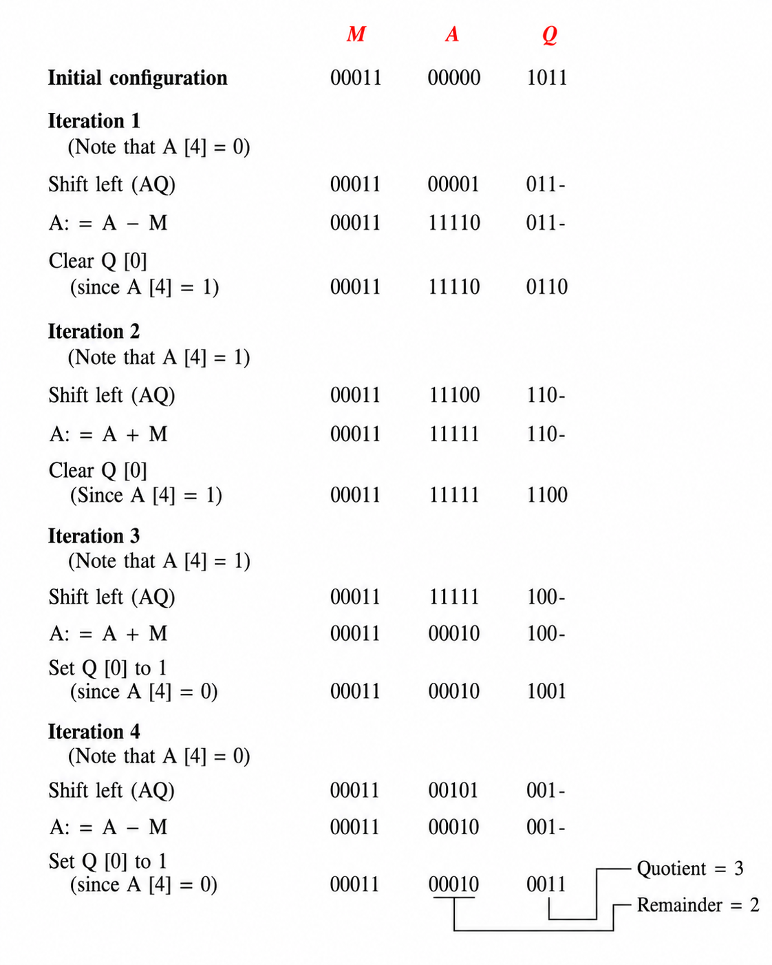
Quotient = 3, Remainder = 2.
In this example, there is no need to restore the remainder, since A register already holds a positive number at the end of the fourth iteration.
Both restoring and nonrestoring division algorithms are derived directly from the paper and pencil method, mechanized using registers M, A, and Q, along with a shift-subtract-restore (or shift-add/subtract) cycle. The restoring algorithm needs an extra addition every time subtraction produces a negative result, while the nonrestoring algorithm removes this need from inside the main loop by merging the restore step into the next iteration's shift-and-operate step, needing only one possible restoration at the very end to recover the correct final remainder. These algorithms may be extended to handle signed integers, if both dividend and divisor are first mapped to positive values, with the sign of the result figured out afterward, similar to the approach used in multiplication.
Q19. Draw the flow chart for floating point multiplication.
Introduction
Floating point numbers are represented using sign, exponent, and mantissa fields, following the standard format \(X = (-1)^S \times M \times 2^{E - Bias}\). Multiplying two floating point numbers needs a proper step-by-step procedure, since sign, exponent, and mantissa must each be handled separately, and the result must be normalized, rounded, and checked for overflow or underflow before it becomes the final answer.
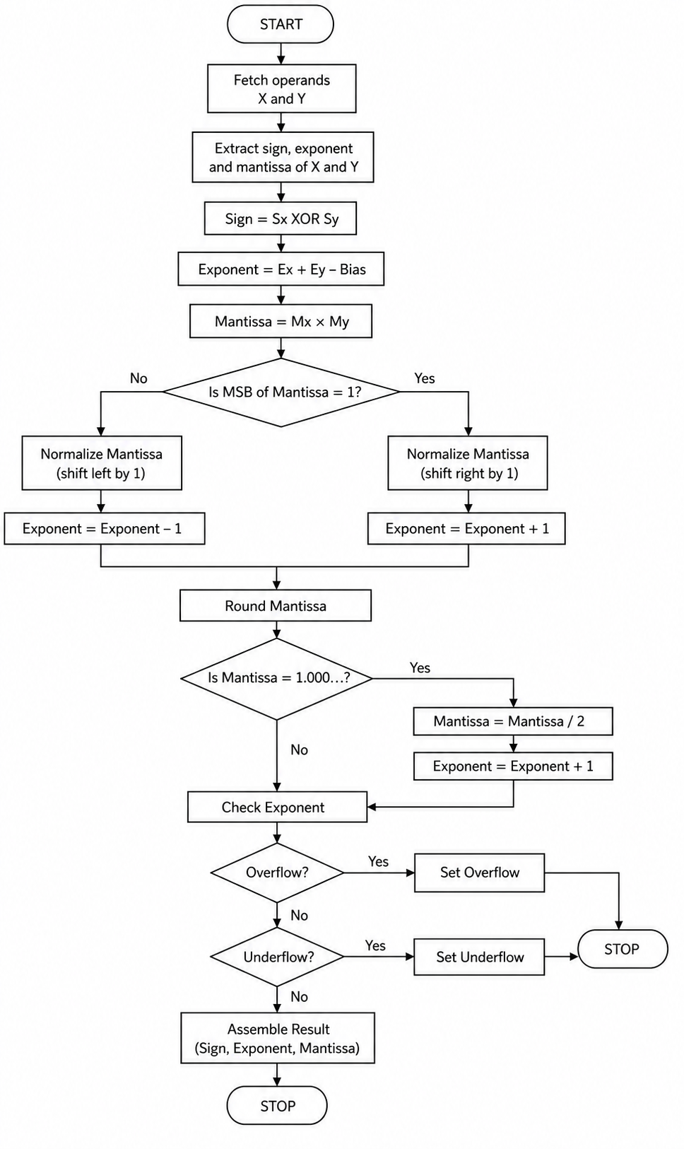
Steps of the Algorithm
The process starts by fetching the two operands X and Y, then extracting their sign, exponent, and mantissa fields separately.
The sign of the result is calculated first, using XOR of the two sign bits:
The exponent of the result is calculated by adding both exponents together and subtracting the bias once, since exponents are stored in biased form and adding two biased exponents directly would leave an extra bias term:
The mantissa of the result is calculated by multiplying both mantissas together:
Since both input mantissas are normalized, meaning each lies in the range \([1, 2)\), their product lies in the range \([1, 4)\), so the result may or may not already be normalized. This is checked by inspecting the most significant bit (MSB) of the mantissa:
- If MSB of mantissa is 1, meaning the product is in range \([2, 4)\), mantissa is normalized by shifting right by 1 bit, and exponent is incremented by 1
- If MSB of mantissa is 0, meaning the product is already less than 2, mantissa is normalized by shifting left by 1 bit, and exponent is decremented by 1
After normalization, the mantissa is rounded to fit within the allowed number of bits. Rounding can sometimes cause the mantissa to become exactly \(2.000...\) due to carry-out, so this is checked separately: if mantissa equals \(1.000...\) after this carry (representing an overflowed value), mantissa is divided by 2 and exponent is incremented by 1 once more, to bring it back into proper normalized range.
Finally, the exponent is checked for overflow and underflow separately. If overflow occurs, an overflow flag is set. If not, underflow is checked, and if it occurs, an underflow flag is set. If neither occurs, the final result is assembled from the calculated sign, exponent, and mantissa, and the process stops.
Flowchart
Example
Suppose \(X_1 = 1.25 \times 2^3\) and \(X_2 = 1.5 \times 2^2\) need to be multiplied.
Sign: assuming both are positive, \(Sign = 0 \oplus 0 = 0\)
Exponent addition:
Mantissa multiplication:
Since \(1.875\) already lies in range \([1,2)\), MSB check shows it is already normalized, so no shifting is needed. Final result:
This can be verified directly, since \(1.25 \times 2^3 = 10\) and \(1.5 \times 2^2 = 6\), and \(10 \times 6 = 60\).
This flowchart shows floating point multiplication as a clear step-by-step hardware procedure, where sign is computed by XOR, exponent by addition with bias correction, and mantissa by direct multiplication, followed by a normalization check, rounding, a possible renormalization due to rounding carry-out, and finally overflow and underflow checks before assembling the result. This complete version is important for a proper exam answer, since it captures the bias handling and rounding-carry edge case that simpler flowcharts often leave out.
Q20. Explain the single cycle datapath for MIPS implementation.
Introduction
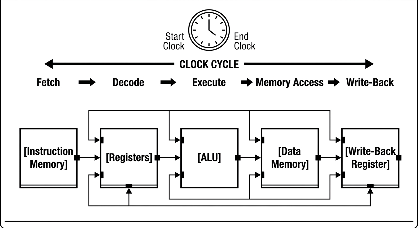
Single cycle data path means, in this type of MIPS design, every instruction gets completed in just one single clock cycle, no matter how simple or complex that instruction is. Because of this, the clock cycle time has to be long enough to handle even the slowest instruction, since all instructions are sharing the same fixed cycle length. Different instructions use different parts of the same hardware, and this is controlled properly using multiplexers and control signals coming from a control unit.
Main Components of the Datapath
Following are the major components used in building this data path:
- Instruction memory: stores all the instructions, and it is accessed using PC as the address, to give out the 32-bit instruction
- Program counter (PC): a register that holds the address of the current instruction, and it gets updated in every cycle
- Register file: contains all 32 general purpose registers, and it can read two registers and write into one register, all within the same cycle
- ALU: performs arithmetic and logic operations, and it is also used to calculate memory addresses and branch target addresses
- Data memory: used only by load and store instructions, for reading from memory or writing into memory
- Sign extend unit: extends the 16-bit immediate value into a full 32-bit value, needed mainly for I-type instructions
- Multiplexers (MUX): placed at different points in the data path, to select the correct signal depending on which instruction type is running
- Control unit: generates all the required control signals, based on opcode field (and
functfield, for R-type instructions)
Instruction Fetch
At the beginning of every cycle, PC is sent to instruction memory, and this fetches the 32-bit instruction stored at that address. At the same time, a separate adder increases PC by 4, so it can point to the next instruction:
R-type Instructions
For R-type instructions like add, sub, and, or, the two source registers, rs and rt, come directly from the fetched instruction, and their values are read from the register file. Both values go into the ALU, where the actual operation gets decided using the funct field, through the control unit. The ALU then produces the result, which is written back into destination register rd.
Load and Store Instructions
For a load instruction like lw, register rs gives the base address, and the immediate field is sign-extended to 32 bits. Both of these go into the ALU, and they get added together to calculate the memory address:
This computed address is then sent to data memory, and the value read from there gets written into register rt. For a store instruction like sw, the same address is calculated the same way, but instead of reading, the value from register rt gets written into data memory at that address.
Branch Instructions
For branch instructions like beq, two registers rs and rt are read and compared inside the ALU, and this produces a zero flag if both values are equal. At the same time, a separate adder calculates the branch target address, by adding the sign-extended and left-shifted immediate value to \(PC + 4\):
Depending on the zero flag from ALU and the branch control signal together, a multiplexer decides whether PC should be updated with this branch target address, or should simply continue with \(PC + 4\) as usual.
Role of Multiplexers
Since different instructions need slightly different paths through the same shared hardware, multiplexers are placed at important points:
- One MUX chooses between rt and immediate value, as second input to ALU, depending on whether instruction is R-type or I-type
- One MUX chooses between ALU result and data memory output, as the value that finally gets written back into register file, depending on whether instruction is load or a normal ALU operation
- One MUX chooses between rt and rd, as destination register, depending on instruction type
- One MUX chooses between \(PC+4\) and branch target address, as next value of PC, depending on whether branch is taken or not
Control Unit
The control unit reads opcode field of the fetched instruction, and based on that, it generates all necessary control signals for that particular instruction, such as RegDst, ALUSrc, MemtoReg, RegWrite, MemRead, MemWrite, Branch, and ALUOp. All these signals control every multiplexer and every read/write enable line inside the datapath, and this makes sure the correct path gets activated automatically, depending on which instruction is currently running.
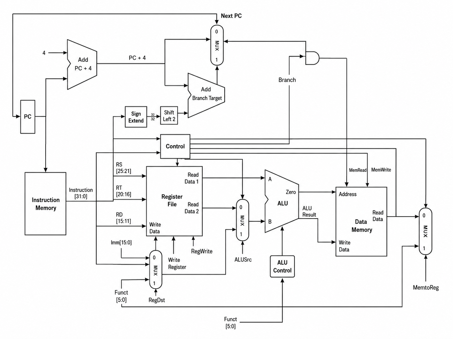
In simple words, the single cycle data path connects instruction memory, register file, ALU, data memory, and PC logic all together, using multiplexers that are controlled by the control unit, so that this one single shared hardware path can correctly handle R-type, load-store, and branch instructions, each within just one clock cycle. Even though this design is quite easy to understand and build, its main problem is that clock cycle time gets fixed according to the slowest instruction, which is usually load word, so even a fast and simple instruction like add ends up wasting time, waiting for the full clock cycle to finish. This is exactly why pipelined and multi-cycle designs are considered more efficient compared to single cycle implementation.
Q21. Write down the steps of designing a microprocessor.
Answer:
Designing a microprocessor is not a single-step task, rather it is a long process that goes through several well-defined stages, starting from understanding what the processor needs to do, all the way down to actual physical chip fabrication. Each step builds on top of the previous one, and mistakes made early in the process become very expensive to fix later, so proper planning at every stage is important.
Step 1: Specification
The first step is deciding the specification of the processor, meaning what the processor is expected to do. This includes deciding the instruction set architecture (ISA), word size (like 32-bit or 64-bit), target clock speed, power consumption limits, and the intended application area, for example whether it is meant for embedded devices, general purpose computers, or high performance servers.
Step 2: Architecture Design
Once specification is decided, the next step is designing the overall architecture, meaning deciding the high-level organization, such as whether the processor will be single cycle, multi-cycle, or pipelined, how many pipeline stages it will have, what kind of memory hierarchy it will use, whether it will support superscalar execution, and how many registers and what addressing modes it will support.
Step 3: Instruction Set Design
At this stage, the actual instruction formats are finalized, deciding things like opcode length, number of registers, addressing modes, and how instructions like R-type, I-type, and J-type (similar to MIPS format discussed earlier) will be encoded into fixed bit patterns.
Step 4: Datapath Design
In this step, all the hardware components needed to execute instructions are designed and connected together, including ALU, register file, memory units, multiplexers, and adders, forming what is known as the datapath. This is where decisions like single cycle datapath versus pipelined datapath (as discussed in the previous question) are actually implemented.
Step 5: Control Unit Design
Once the datapath is ready, the control unit is designed, whose job is to generate proper control signals for every instruction, so that the datapath behaves correctly for each instruction type. Control unit can either be hardwired, using logic gates directly, or microprogrammed, using stored microcode, depending on the design philosophy chosen (this connects back to the RISC vs CISC discussion from earlier).
Step 6: Logic Design
At this stage, the architecture and control design are converted into actual digital logic circuits, such as combinational and sequential circuits, using gates, flip-flops, multiplexers, and adders, to physically realize every part of the data path and control unit designed in previous steps.
Step 7: Circuit Design
Here, the logic gates designed in the previous step are converted into actual transistor-level circuits, deciding exact transistor sizes, arrangement, and timing characteristics, keeping in mind speed, power consumption, and area constraints.
Step 8: Physical Design and Layout
In this step, the transistor circuits are converted into an actual physical layout, meaning the exact placement of transistors and wiring on the silicon chip is decided, keeping fabrication rules and constraints in mind, so that it can be manufactured properly.
Step 9: Verification and Testing
Before actual fabrication, the entire design is thoroughly simulated and verified at every level, checking that the logic behaves correctly, timing constraints are met, and the design matches original specifications. This includes functional verification, timing verification, and power analysis, since any error found after fabrication becomes extremely costly to fix.
Step 10: Fabrication
Once verification is complete, the design is sent for actual fabrication, where the chip is physically manufactured using semiconductor processes, like photolithography and doping, on a silicon wafer, following the physical layout designed earlier.
Step 11: Testing and Validation
After fabrication, the actual manufactured chips are tested physically, to check whether they work correctly as intended, and to catch any manufacturing defects, before the processor is finally released for real-world use.
Flow Summary
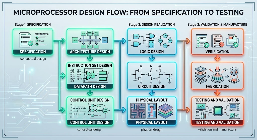
Designing a microprocessor is a long, layered process, moving step by step from a high-level idea of what the processor should do, all the way down to a physical, fabricated, and tested silicon chip. This process directly connects back to the layered computing system architecture discussed in an earlier question, since each step here, like ISA design, data path design, and logic design, actually corresponds to moving down through those same abstraction layers, one at a time, from software-visible architecture down to physical hardware.
Q22. Explain the implementation of jump instruction in MIPS.
Answer:
Jump instruction in MIPS, like j or jal, is used for unconditional transfer of control to a new address, unlike branch instructions which depend on a condition. Since jump does not need any comparison, it only needs the target address to be correctly calculated and loaded into PC, and this is implemented using the J-type instruction format along with pseudo-direct addressing, as discussed in earlier questions.
J-type Instruction Format
Jump instructions use the J-type format, which has only two fields:
Here, opcode identifies whether the instruction is j or jal, and the 26-bit address field holds most of the target address, but this alone is not enough to represent a full 32-bit address, so extra bits must be added from elsewhere.
How the Target Address is Calculated
Since MIPS instructions are always word-aligned, meaning every instruction address is a multiple of 4, the lowest 2 bits of any instruction address are always 0, and these do not need to be stored explicitly. So the 26-bit address field represents only bits 27 down to 2 of the actual target address.
To get the complete 32-bit jump address, following steps are done:
- The 26-bit address field from the instruction is shifted left by 2 bits, which effectively appends two zero bits at the end, giving a 28-bit value
- The top 4 bits (bits 31 to 28) are taken directly from the current value of \(PC + 4\), since jump instructions cannot reach addresses outside this same 256 MB region
This can be written as:
Here, the symbol \(\{ \}\) means these three parts are concatenated together to form the final 32-bit address.
Data path Implementation
In the single cycle data path, implementing jump needs a few additional hardware pieces on top of the normal data path discussed earlier:
- The 26-bit address field from the instruction is taken and shifted left by 2 bits using simple wiring (no actual shifter circuit is needed, since this is just appending two zero bits)
- The top 4 bits of \(PC + 4\) are taken directly using wiring, and concatenated with the shifted address field, to form the full 32-bit jump target
- A multiplexer is placed before the PC register, which selects between three possible values: \(PC + 4\) (normal sequential execution), branch target address (for conditional branches), or this newly calculated jump target address (for jump instructions)
- The control unit generates a Jump control signal, which is set to 1 only when the instruction is j or jal, and this signal controls the final multiplexer, forcing PC to load the jump target address instead of any other value
Example
Suppose the instruction j 1024 is being executed, and current \(PC + 4 = 0x00400004\).
The address field in the instruction holds the value 1024 (in the 26-bit field). Shifting this left by 2 gives:
Top 4 bits of \(PC + 4\), which is \(0x00400004\), are \(0000\) (since the address starts with 0x0...).
So final jump target becomes:
This value gets loaded directly into PC, and execution continues from this new address in the next cycle.
Difference for jal
The jal instruction (jump and link) works exactly the same way for calculating the jump target, but it has one extra step: before jumping, it saves the return address, which is \(PC + 4\) (the address of the instruction right after jal), into register $31 (also called $ra). This is done using an extra write into the register file, alongside the normal jump target calculation, and this is what allows the program to return back to this point later, using a jr $ra instruction, making jal useful for implementing function calls.
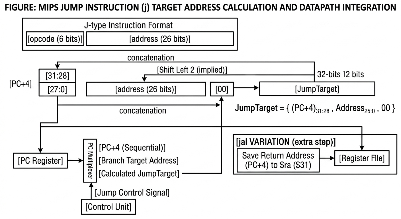
Jump instruction implementation in MIPS relies on the J-type format's 26-bit address field, combined with the upper 4 bits of \(PC + 4\) and two appended zero bits, to form the complete 32-bit target address, and this calculated address is loaded directly into PC using a dedicated multiplexer controlled by the Jump signal. Since jump does not need any ALU comparison like branch does, its implementation is comparatively simpler, needing only wiring and concatenation logic, rather than actual arithmetic computation, and the jal variant additionally saves the return address into register $31, making function calls possible in MIPS assembly.
Q23. How does the pipeline increase the performance of processor? Explain.
Answer:
Pipelining is a technique used in processor design, where execution of an instruction is broken down into multiple smaller stages, and these stages overlap with stages of other instructions, similar to how work is done on an assembly line in a factory. Instead of waiting for one instruction to completely finish before starting the next one, pipelining allows multiple instructions to be in different stages of execution at the same time, and this overlapping is exactly what improves overall performance.
Basic Idea Behind Pipelining
In a non-pipelined (single cycle) processor, one complete instruction must finish entirely before the next instruction can even start, so every instruction, whether simple or complex, takes the same long clock cycle to complete. In a pipelined processor, execution of an instruction is divided into separate stages, for example fetch, decode, execute, memory access, and write back, and each stage is handled by a separate hardware unit. While one instruction is being decoded, the next instruction can already be fetched at the same time, and while that instruction is being executed, yet another instruction can be fetched, and so on. This way, multiple instructions move through the pipeline simultaneously, each at a different stage.
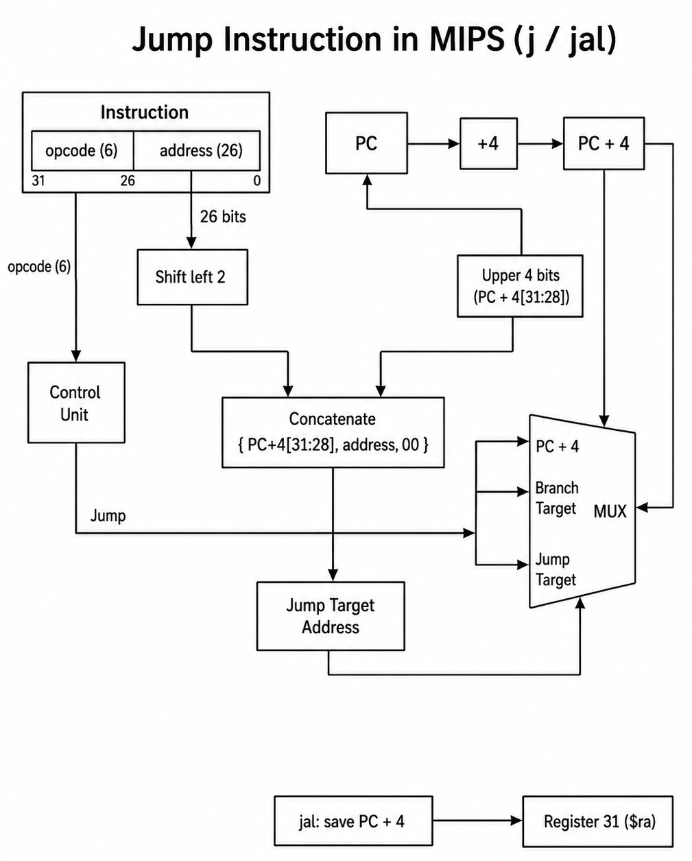
How Pipeline Improves Performance
In a non-pipelined design, if a complete instruction takes time \(T\), then \(n\) instructions will take approximately:
In an ideal pipeline with \(k\) stages, each stage takes time \(\frac{T}{k}\), and instructions overlap in execution, so the total time becomes approximately:
Here, the first instruction still takes full time \(T\) to go through all \(k\) stages, but every instruction after that only adds one extra stage time \(\frac{T}{k}\), since it overlaps with the previous instructions already inside the pipeline.
For a large number of instructions, this gives an ideal speedup close to:
meaning, in the best case, a \(k\)-stage pipeline can make the processor almost \(k\) times faster compared to a non-pipelined design, since the clock cycle time is now based only on the slowest single stage, not the entire instruction.
Why This Happens
The main reason pipelining improves performance is that it increases instruction throughput, meaning more instructions get completed per unit time, even though the time taken to complete a single individual instruction (called latency) does not really decrease, and in fact latency can even slightly increase due to pipeline overhead. But since multiple instructions are being processed simultaneously at different stages, the overall rate at which instructions finish becomes much higher.
Example
Suppose a single instruction takes 500 ps to complete in a non-pipelined processor, and this same instruction is broken into 5 pipeline stages of 100 ps each.
For 100 instructions, non-pipelined time:
For pipelined execution:
So pipelining reduces total execution time from 50000 ps to 10400 ps, which is close to the ideal 5 times speedup expected from a 5-stage pipeline.
Limitations
Even though pipelining greatly improves performance, ideal speedup of exactly \(k\) times is rarely achieved in practice, because of pipeline hazards, such as structural hazards, data hazards, and control hazards (these will be discussed in detail in later questions), which can force the pipeline to stall, reducing the actual achieved speedup below the theoretical ideal value.
Pipelining increases processor performance mainly by increasing instruction throughput, allowing multiple instructions to overlap and execute simultaneously across different stages, instead of waiting for each instruction to fully complete one at a time. Even though individual instruction latency does not reduce, and pipeline hazards prevent the ideal speedup from being fully achieved in real designs, pipelining still remains one of the most important and widely used techniques for improving processor performance without needing to increase clock frequency or duplicate hardware entirely.
Q24. Write down the stages of pipeline in MIPS architecture.
Answer:
MIPS pipeline breaks down the execution of every instruction into five separate stages, and this design is often called the classic 5-stage MIPS pipeline. Each stage is handled by a different hardware unit, and at any given moment, five different instructions can be present inside the pipeline together, each one at a different stage, following the overlapping concept discussed in the previous question.
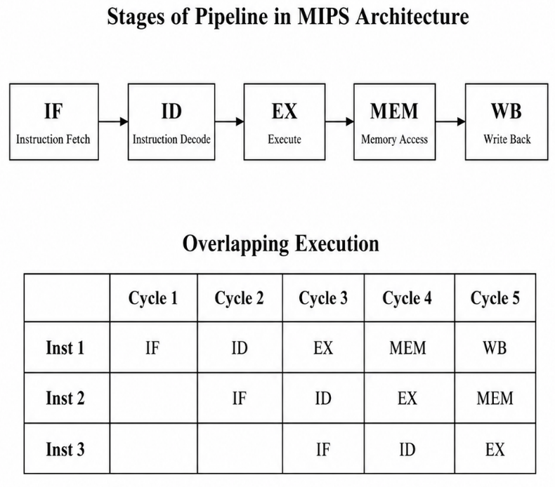
The Five Pipeline Stages
IF (Instruction Fetch)
In this stage, the instruction is fetched from instruction memory, using the current value of PC as the address. At the same time, PC is updated to \(PC + 4\), to point to the next instruction for the following cycle.
ID (Instruction Decode / Register Fetch)
In this stage, the fetched instruction is decoded, meaning opcode and register fields are identified, and the required source registers are read from the register file. The 16-bit immediate field, if present, is also sign-extended to 32 bits in this stage, and control signals for later stages are generated here as well.
EX (Execute)
In this stage, the actual computation happens inside the ALU. For R-type instructions, this means performing the arithmetic or logic operation on the two register values. For load and store instructions, this means calculating the effective memory address, by adding base register value with the sign-extended offset. For branch instructions, this means comparing the two register values to decide whether the branch should be taken.
MEM (Memory Access)
In this stage, data memory is accessed, but only load and store instructions actually use this stage meaningfully. For a load instruction, data is read from memory at the address calculated in EX stage. For a store instruction, data is written into memory at that address. R-type instructions simply pass through this stage without doing anything, since they don't need memory access.
WB (Write Back)
In this final stage, the result is written back into the register file. For R-type instructions, this is the ALU result. For load instructions, this is the value read from memory in the MEM stage. Branch and store instructions do not need this stage, since they don't produce a value that needs to be written into a register.
Pipeline Stage Summary Table
| Stage | Full Name | Main Work Done |
|---|---|---|
| IF | Instruction Fetch | Fetch instruction from memory, update PC |
| ID | Instruction Decode | Decode instruction, read registers, sign-extend immediate |
| EX | Execute | ALU operation, address calculation, or branch comparison |
| MEM | Memory Access | Read or write data memory (load/store only) |
| WB | Write Back | Write result back into register file |
How Instructions Overlap Across Stages
Since each stage is a separate hardware unit, multiple instructions can occupy different stages at the same time, and this can be shown using a pipeline timing diagram:
| Instruction | Cycle 1 | Cycle 2 | Cycle 3 | Cycle 4 | Cycle 5 |
|---|---|---|---|---|---|
| Instruction 1 | IF | ID | EX | MEM | WB |
| Instruction 2 | IF | ID | EX | MEM | |
| Instruction 3 | IF | ID | EX |
Here, while instruction 1 is in EX stage during cycle 3, instruction 2 is simultaneously in ID stage, and instruction 3 is simultaneously in IF stage, all inside the same clock cycle, showing exactly how overlapping execution takes place.
The MIPS pipeline uses five stages, IF, ID, EX, MEM, and WB, and each instruction moves through these stages one by one, while overlapping with other instructions that are simultaneously present at different stages. This design directly connects back to the single cycle datapath discussed earlier, since the same major hardware components, that is instruction memory, register file, ALU, data memory, and the write-back path, are essentially the same components, just now separated into distinct stages using pipeline registers between them, allowing multiple instructions to be processed in parallel rather than one complete instruction finishing before the next one begins.
Q25. What do you mean by structural hazard, data hazard and control hazard?
Answer:
Hazards in pipelining are situations where the next instruction cannot execute properly in its designated clock cycle, because of some conflict or dependency created by the pipelining process itself. These hazards, if not handled properly, force the pipeline to stall, meaning some instructions have to wait, and this reduces the actual performance gain expected from pipelining. There are three main types of hazards: structural hazard, data hazard, and control hazard.
Structural Hazard
Structural hazard happens when two or more instructions inside the pipeline need to use the same hardware resource at the same time, but that resource is only available once, so both instructions cannot be served simultaneously.
For example, if instruction memory and data memory are combined into a single shared memory unit, then a load instruction, which needs to access memory in its MEM stage, and a different instruction, which needs to fetch a new instruction in its IF stage, might end up needing to access this same shared memory at the same clock cycle. Since only one memory access can happen at a time in a single-ported memory, this creates a structural hazard.
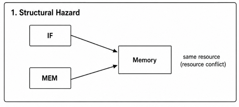
This type of hazard is usually solved by design itself, for example by using separate instruction memory and data memory (following Harvard architecture style), so both accesses can happen simultaneously without conflict.
Data Hazard
Data hazard happens when an instruction depends on the result of a previous instruction that has not yet completed and written its result back, but the pipeline tries to read that value too early, before it becomes available.
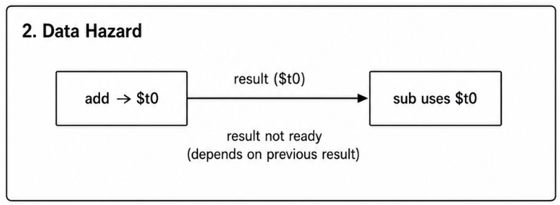
For example, consider this sequence:
Here, the second instruction needs the value of $t0, but $t0 is only calculated by the first instruction, and in a pipeline, the first instruction's result is not written back into the register file until its WB stage, which happens several cycles after the second instruction has already tried to read $t0 in its own ID stage. This mismatch in timing causes a data hazard, since sub might end up reading the old, incorrect value of $t0.
Control Hazard
Control hazard happens because of branch and jump instructions, where the pipeline does not know for certain what the next instruction should be, until the branch decision itself is calculated, but by that time, the pipeline has usually already fetched several following instructions, assuming normal sequential execution.
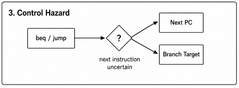
For example, consider this sequence:
Here, the pipeline fetches the add instruction right after beq, assuming the branch is not taken, but if the branch condition actually turns out to be true, this fetched add instruction was wrong, and it must be discarded, causing wasted cycles. This uncertainty about which instruction comes next is exactly what causes a control hazard.
Comparison Table
| Hazard Type | Cause | Example Situation |
|---|---|---|
| Structural Hazard | Same hardware resource needed by two instructions at once | Shared memory for instruction fetch and data access |
| Data Hazard | Instruction needs a value not yet written back by previous instruction | add $t0,... followed immediately by sub ...,$t0,... |
| Control Hazard | Next instruction is uncertain due to branch/jump decision | beq followed immediately by next sequential instruction |
Structural hazard, data hazard, and control hazard are three fundamental problems created by the pipelining technique itself, each one arising from a different reason: hardware resource conflict for structural hazard, data dependency timing for data hazard, and instruction flow uncertainty for control hazard. Understanding these hazards properly is important, because the next question builds directly on this, explaining the actual techniques used to detect and remove these hazards, so the pipeline can keep working efficiently despite these underlying problems.
Q26. How data and control hazard is removed? Explain.
Answer:
Since data hazard and control hazard, discussed in the previous question, can seriously reduce pipeline performance if left unhandled, several techniques have been developed to detect and remove these hazards, so the pipeline can keep working as efficiently as possible. Data hazards are mainly removed using forwarding and stalling, while control hazards are mainly removed using branch prediction and early branch resolution.
Removing Data Hazard
Forwarding (Bypassing)
Forwarding, also called bypassing, is the most common technique used to remove data hazards. Instead of waiting for a value to be written back into the register file in the WB stage, and then read again in a later instruction's ID stage, the result is directly forwarded from the pipeline register right after it is calculated, straight into the input of the ALU for the instruction that needs it.
For example, in this sequence:
The result of add, calculated at the end of EX stage, can be forwarded directly from the EX/MEM pipeline register into the ALU input of sub, during sub's own EX stage, instead of waiting for add to reach its WB stage. This way, sub gets the correct value of $t0 right on time, without needing to stall the pipeline at all.
Stalling (Pipeline Interlock)
In some cases, especially with load instructions, forwarding alone is not enough, because the loaded value is only available after the MEM stage, not after EX stage. This situation is called a load-use hazard.
For example:
Here, add needs $t0 in its EX stage, but lw only produces this value at the end of its own MEM stage, which is too late even for forwarding to help completely. In this case, the pipeline must insert a stall (also called a bubble), meaning the add instruction is held back for one cycle, so that its EX stage happens one cycle later, giving enough time for the loaded value to become available and get forwarded properly.
Removing Control Hazard
Branch Prediction
Branch prediction is a technique where the pipeline makes a guess about whether a branch will be taken or not, and continues fetching instructions based on this guess, instead of simply stalling and waiting for the branch decision to be known for certain. If the prediction turns out correct, no time is wasted at all. If the prediction turns out wrong, the wrongly fetched instructions are discarded (this is called a pipeline flush), and correct instructions are fetched instead. This technique is discussed in more detail in the next question.
Early Branch Resolution
Another simple technique is to move the branch decision earlier in the pipeline, for example calculating the branch condition and target address during the ID stage itself, instead of waiting until the EX stage. This reduces the number of wrongly fetched instructions in case the branch turns out to be taken, since fewer instructions get fetched incorrectly before the branch outcome becomes known.
Delayed Branch
Delayed branch is a technique specific to some MIPS implementations, where the instruction immediately following a branch (called the branch delay slot) is always executed, regardless of whether the branch is taken or not. The compiler is made responsible for filling this delay slot with a useful, independent instruction, so this slot is not wasted, and the pipeline does not need to stall or flush for this one cycle at all.
Comparison Table
| Hazard Type | Technique Used | How It Works |
|---|---|---|
| Data Hazard | Forwarding | Result passed directly from pipeline register to ALU input, skipping register file |
| Data Hazard | Stalling | Pipeline bubble inserted when forwarding alone is not enough (load-use case) |
| Control Hazard | Branch Prediction | Guess branch outcome, flush pipeline only if guess is wrong |
| Control Hazard | Early Branch Resolution | Calculate branch decision earlier (in ID stage) to reduce wasted fetches |
| Control Hazard | Delayed Branch | Always execute instruction in branch delay slot, filled by compiler |
Data hazards are mainly removed using forwarding, and stalling is used only when forwarding alone cannot solve the timing problem, such as in load-use hazard cases. Control hazards are mainly removed using branch prediction, along with supporting techniques like early branch resolution and delayed branch, which reduce the number of wasted cycles caused by incorrect instruction fetching after a branch. Together, these techniques allow a pipelined processor to stay close to its ideal performance, even though data dependencies and branch instructions naturally try to break the smooth overlapping flow of instructions through the pipeline.
Q27. What is branch prediction? Explain with example.
Introduction
Branch prediction is a technique used in pipelined processors to guess the outcome of a branch instruction, that is whether the branch will be taken or not taken, before the actual branch condition is fully evaluated. Since control hazards happen exactly because the pipeline does not know which instruction comes next until the branch is resolved, branch prediction allows the pipeline to keep fetching and executing instructions based on a guess, instead of simply stalling and wasting clock cycles while waiting for the real outcome.
Why Branch Prediction is Needed
In a pipelined processor, by the time a branch instruction reaches the stage where its condition is actually evaluated (for example the EX stage in classic MIPS pipeline), several following instructions have already been fetched into the pipeline, assuming normal sequential execution. If the branch turns out to be taken, all these fetched instructions are wrong, and must be discarded, causing wasted cycles, called a pipeline flush. Branch prediction tries to reduce how often this flush happens, by making an intelligent guess about the branch outcome as early as possible.
Types of Branch Prediction
Static Branch Prediction
Static prediction makes a fixed guess that does not change during program execution, and is usually decided at compile time or by a simple fixed rule. Common static prediction strategies include:
- Predict not taken, meaning pipeline always assumes branch will not be taken, and continues fetching the next sequential instruction
- Predict taken, meaning pipeline always assumes branch will be taken, and starts fetching from the branch target address directly
- Backward taken, forward not taken (BTFNT), meaning branches that jump backward (like loop branches) are predicted taken, while branches that jump forward are predicted not taken, since loop branches are usually taken most of the time
Dynamic Branch Prediction
Dynamic prediction makes its guess based on the actual runtime behavior of the branch, usually by keeping track of how that branch behaved in its previous few executions, and this guess can change as the program runs. A common method is using a 2-bit saturating counter, stored for each branch, which can be in one of four states: strongly not taken, weakly not taken, weakly taken, and strongly taken. Every time the branch is actually taken, the counter moves one step toward "strongly taken", and every time it is not taken, the counter moves one step toward "strongly not taken". The prediction for next time is based on whichever side (taken or not taken) the counter currently leans toward.
Example
Suppose a loop runs 5 times, using following instruction pattern:
Using static "predict taken" strategy, since this branch usually keeps looping back for the first 4 iterations, prediction will be correct 4 times, and it will only be wrong once, on the final iteration when the loop actually exits and branch is not taken. This gives \(4/5 = 80\%\) prediction accuracy for this particular loop.
Using dynamic 2-bit counter, suppose counter starts at "weakly taken" state. Since the branch keeps getting taken repeatedly for the first few iterations, counter quickly moves to "strongly taken" state, and stays correctly predicted as taken for iterations 2, 3, and 4. Only on the last iteration, when loop actually exits, prediction turns out wrong, but this single misprediction does not immediately flip the counter's prediction for next time this same branch runs elsewhere in the program, since the 2-bit counter needs two consecutive wrong guesses before it fully switches its prediction.
Misprediction Penalty
Whenever a prediction turns out wrong, all instructions that were fetched based on that wrong guess must be discarded from the pipeline, and correct instructions must be fetched instead, starting from the correct address. This wasted time is called the misprediction penalty, and it becomes larger in deeper pipelines, since more instructions get fetched incorrectly before the mistake is even detected.
Branch prediction is an important technique for reducing the performance loss caused by control hazards, by making an educated guess about branch outcomes ahead of time, instead of forcing the pipeline to stall until the real outcome is known. Static prediction uses fixed, simple rules decided beforehand, while dynamic prediction adapts based on actual runtime behavior of each branch, usually using counters like the 2-bit saturating counter, and this adaptability generally makes dynamic prediction more accurate for real programs, especially ones with loops, where branch behavior tends to follow a repeating pattern.