12 EEE lab 02
Experiment No. 02
Name of the Experiment: Observation of Characteristics of a Zener Diode
1. Objectives
- To study the I–V characteristics of a Zener diode in forward and reverse bias.
- To determine the Zener breakdown voltage (\(V_z\)).
- To analyze the application of a Zener diode as a voltage regulator.
2. Apparatus Required
- Zener diode (D1N750, ~6.2 V)
- DC regulated power supply (0–20 V)
- Resistors: 100 Ω (series), 1 kΩ, 10 kΩ, etc.
- Breadboard
- Two multimeters (for current and voltage measurement)
- Connecting wires
3. Theory
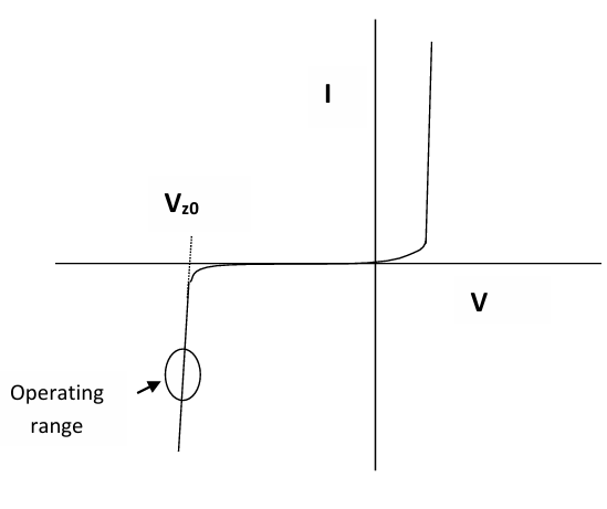
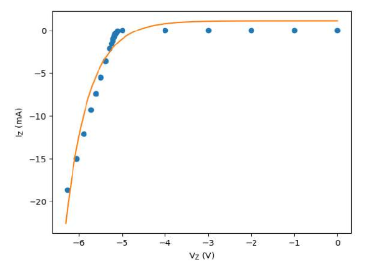
A diode which is different from the conventional semiconductor diode is the Zener diode. The Zener diode's forward-biased characteristic is the same as that of a conventional diode. But, the reverse bias characteristic is the same as an ordinary diode up to a specific value known as the Zener voltage. An attempt to increase the reverse bias voltage beyond the Zener voltage results only in an increase in the reverse current and the diode voltage tends to remain constant ( see Fig.1).
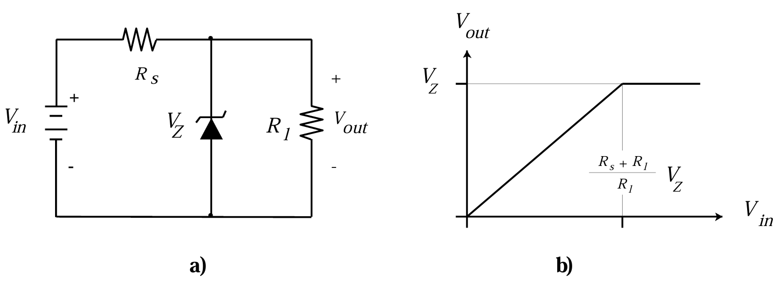
The I-V characteristic of a Zener Diode is shown in Fig. 2. In the forward bias region, it is very similar to an ordinary diode (p-n junction). In the reverse bias region, there is Zener breakdown which limits the voltage to Vz. The operating region shown in Fig. 2 is where voltage regulation is effective. In other words, the output would be limited to Vz even if input exceeds it. At any point in the operating range, an incremental resistance rz can be defined as follows.
Incremental resistance (\(r_z\)):
Here, \(\Delta V\) and \(\Delta I\) represent the change in voltage and current, respectively, in the operating region. The value of \(r_z\) can be readily obtained from the slope of the V–I curve in this region. Another important parameter is line regulation, which indicates how effective the regulator is in maintaining the output voltage close to \(V_Z\) and suppressing ripple or noise. It is defined as follows:
Line regulation:
Here, ΔVo and ΔVin are fluctuation in output and input voltage respectively. One can measure these two quantities and then determine line regulation. A theoretical analysis gives the following expression for line regulation.
Line Regulation:
Here \(r_z\) is defined in equation (1) and \(R_s\) is shown in Fig. 1. If there is load attached to the output then \(r_z\) should be replaced by
Here \(R_L\) is the load.
4. Procedure
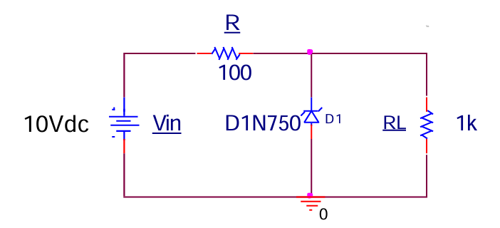
- Construct the circuit as shown in Fig. 3 with series resistance of 100 Ω and the Zener diode in reverse bias.
- Vary the DC input voltage gradually and measure the diode voltage and current.
- Record readings until the diode clearly enters breakdown region.
- Tabulate the values of voltage (V) and current (I).
- Plot the V–I graph and mark the Zener breakdown voltage (\(V_z\)).
- Repeat with different load resistances (\(R_L\)) to observe Zener regulator action.
- Record \(V_o\), \(I_L\), and \(I_Z\).
- Analyze how the Zener maintains constant output voltage despite load variation.
5. Observations
a) Reverse Bias Characteristics
| Serial No. | Voltage \(V_Z\) (V) | Current \(I_Z\) (mA) |
|---|---|---|
| 1 | 0.00 | 0.000 |
| 2 | 1.00 | 0.000 |
| 3 | 2.00 | 0.000 |
| 4 | 3.00 | 0.000 |
| 5 | 4.00 | 0.000 |
| 6 | 5.00 | 0.000 |
| 7 | 5.20 | 0.100 |
| 8 | 5.40 | 0.265 |
| 9 | 5.60 | 0.442 |
| 10 | 5.80 | 0.623 |
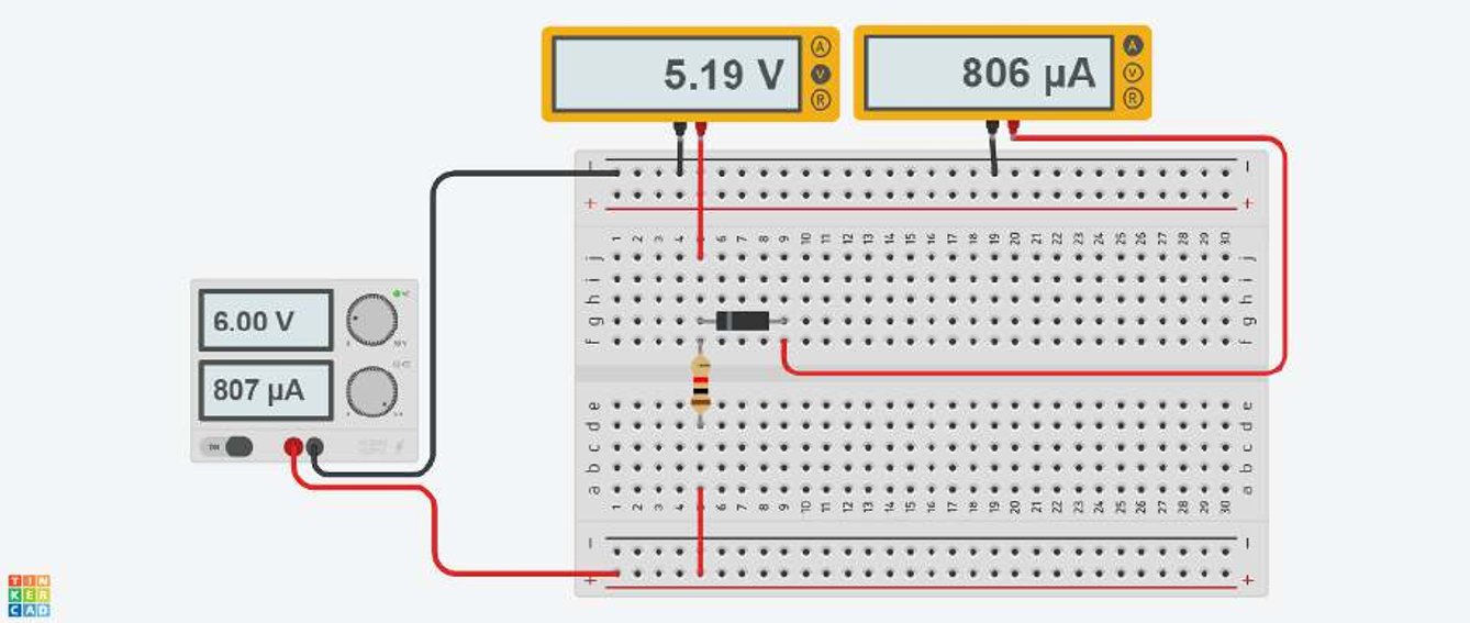
| 11 | 6.00 | 0.806 |
| 12 | 6.20 | 0.991 |
| 13 | 6.40 | 1.180 |
| 14 | 6.80 | 1.550 |
| 15 | 7.40 | 2.110 |
| 16 | 9.00 | 3.610 |
| 17 | 11.00 | 5.500 |
| 18 | 13.00 | 7.390 |
| 19 | 15.00 | 9.280 |
| 20 | 18.00 | 12.100 |
| 21 | 21.00 | 15.000 |
| 22 | 25.00 | 18.700 |
On plotting, breakdown observed at:
b) Zener Regulator Table:
| \(R_L\) | \(V_O\) (V) | \(I_L\) (mA) | \(I_Z\) (mA) |
|---|---|---|---|
| 10 kΩ | 6.05 | 0.605 | 38.9 |
| 1 kΩ | 6.05 | 6.05 | 33.5 |
| 100 Ω | 5.00 (no regulation) | 50.0 | ~0 |
| 10 Ω | 0.909 (no regulation) | 90.9 | ~0 |
- Series resistor \(R_s = 100\,\Omega\)
- Input \(V_{in} = 10\,\text{V}\) (shown in the figure)
- Measured Zener voltage in regulation: \(V_Z \approx 6.05\,\text{V}\) (from your table around \(I_Z=15\) mA)
Supply current while regulating:
When regulating:
If \(I_L\ge I_S\) the Zener turns off and the node follows a divider:
2(i) Comment & explanation
- For 10 kΩ → 1 kΩ, \(V_O\) stays ≈ 6.05 V while \(I_Z\) adjusts so that \(I_L+I_Z=I_S\). This is regulation action.
- For 100 Ω and 10 Ω, the load current demand \(I_L\) exceeds \(I_S\), the Zener can’t conduct, turns off, and \(V_O\) drops per the resistor divider—regulation fails.
2(ii) Breakdown voltage & smallest regulating load
- From your measurements: \(\boxed{V_Z \approx 6.05\ \text{V (at}\ \sim15\,\text{mA})}\)
- Minimum load that still regulates:
(≈ 150 Ω in standard values). Loads smaller than ~150 Ω will pull too much current and the Zener can’t regulate.
6. Result
- The breakdown voltage of the Zener diode is found to be:
- Zener diode maintains nearly constant voltage in breakdown region, confirming its use as a regulator.
7. Discussion
Precautions:
* Avoid excessive current to prevent diode damage.
* Increase supply gradually.
* Observe polarity carefully.
* In regulator mode, the output voltage remains almost unchanged for different \(R_L\), as long as the diode stays in breakdown region.
* For very small \(R_L\), load current increases too much and Zener may fail to regulate.