Defects In Solid
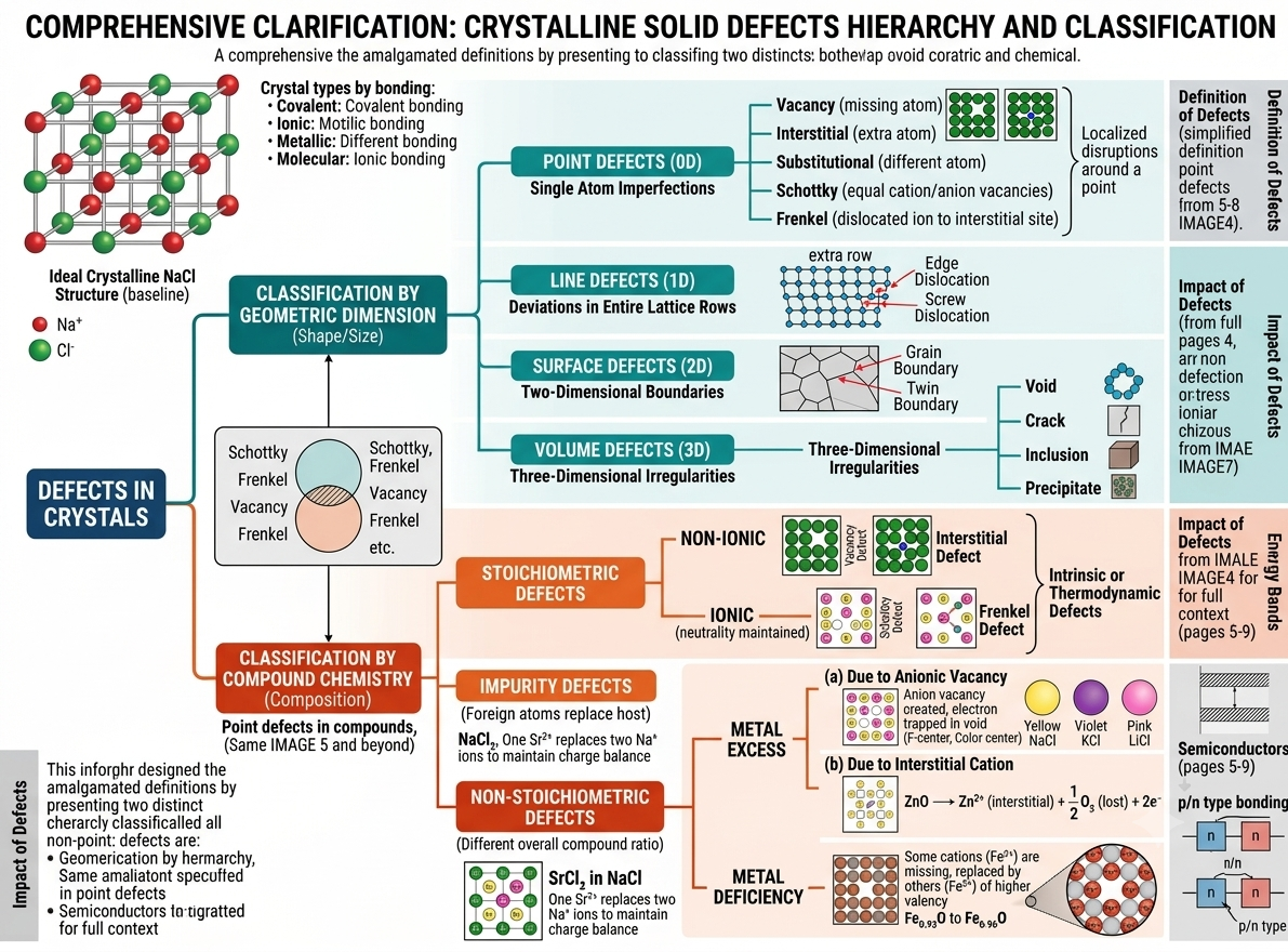
Exam Study Notes: Additional Crucial Terminologies
1. Band Theory of Solids
-
Energy Band (শক্তি ব্যান্ড / পট): When individual atoms pack closely together to form a solid crystal, the outer electrons are heavily influenced (প্রভাবিত) by the electrostatic fields of neighboring atoms. Instead of possessing a single, discrete energy level like an isolated atom, the electrons share a continuous range or spread of closely spaced energy levels, which is defined as an energy band.
-
Valence Band (যোজন ব্যান্ড): This is the highest energy band containing the valence electrons that reside in the outermost orbit of the constituent atoms. This band can be completely or partially filled with electrons depending on the material, but it is never fully empty.
-
Conduction Band (পরিবহন ব্যান্ড): This is the higher-energy electronic band containing free valence electrons that have detached (বিচ্ছিন্ন) from the attractive forces of the nucleus. These free electrons travel through the lattice and actively participate in conducting electric current.
-
Forbidden Energy Gap (নিষিদ্ধ শক্তি ব্যবধান): This is the empty energy region separating the valence band from the conduction band where no permitted quantum energy states exist. No electron can physically occupy this region. To lift an electron from the valence band to the conduction band, external energy equal to this forbidden gap must be supplied.
2. Classification of Materials based on Conductivity
-
Insulator (অান্তরক / অপরিবাহী): A material through which electric current cannot flow due to an extremely high specific resistance (আপেক্ষিক রোধ) of the order of \(10^{12}\text{ }\Omega\text{m}\). In an insulator, the conduction band is completely empty, and the forbidden energy gap is exceptionally wide, measuring about \(6\text{ eV}\) to \(15\text{ eV}\).
-
Conductor (পরিবাহী): A material featuring a massive density of free conduction electrons through which electric current passes effortlessly. Its specific resistance is extremely low, about \(10^{-8}\text{ }\Omega\text{m}\), because the valence band and conduction band overlap (একে অপরের ওপর আপতিত হওয়া) each other, keeping the forbidden energy gap at zero.
-
Semiconductor (অর্ধপরিবাহী): A unique class of solid substances whose specific resistance falls between conductors and insulators, approximately around \(10^{-4}\text{ }\Omega\text{m}\). Their electrical conductivity increases drastically with an increase in temperature or by the deliberate addition of specific impurities, and their forbidden energy gap is less than \(1.1\text{ eV}\).
3. Semiconductor Doping and Carrier Dynamics
-
Doping (ডোপিং / অপমিশ্রণ): The deliberate process of adding a tiny, controlled fraction of specific foreign impurities (typically about one impurity atom in \(10^8\) host atoms) to a pure semiconductor to highly elevate its electrical conductivity.
-
Intrinsic Semiconductor (সহজাত / বিশুদ্ধ অর্ধপরিবাহী): A perfectly pure semiconductor crystal consisting of Group 14 elements (like pure Silicon or Germanium) without any external impurity elements added to it. Their electrical conductivity is low at room temperature because the number of naturally available free charge carriers is very small.
-
Extrinsic Semiconductor (বহির্জাত / অবিশুদ্ধ অর্ধপরিবাহী): A semiconductor whose electrical properties and conductivity have been altered and enhanced by doping it with either trivalent or pentavalent impurity atoms.
-
p-Type Semiconductor (পি-টাইপ অর্ধপরিবাহী): An extrinsic semiconductor formed when a pure crystal is doped with a trivalent impurity element containing 3 valence electrons (like Gallium, Boron, or Indium). This doping introduces a localized electron deficiency, creating a "hole" which acts as the majority charge carrier (প্রধান আধান বাহক).
-
n-Type Semiconductor (এন-টাইপ অর্ধপরিবাহী): An extrinsic semiconductor formed when a pure crystal is doped with a pentavalent impurity element containing 5 valence electrons (like Arsenic, Phosphorus, or Antimony). Four electrons form covalent bonds with the host lattice, while the fifth electron is left completely free to act as a conduction charge carrier.
-
Acceptor Atom (গ্রাহক পরমাণু): The trivalent impurity atom in a p-type semiconductor lattice that actively demands an electron from neighboring atoms to complete its stable chemical bonding configuration.
-
Donor Atom (দাতা পরমাণু): The pentavalent impurity atom in an n-type semiconductor lattice that readily donates (দান করা) its extra fifth valence electron to the conduction band to increase free electron concentration.
-
Hole (গহ্বর / হোল): A vacant, positively charged space left behind in the valence band when a valence electron gains sufficient thermal energy to rupture its covalent bond and escape into the conduction band.
4. Related Crystal Phenomena
-
F-Centre / Color Center (এফ-কেন্দ্র / বর্ণ কেন্দ্র): A unique non-stoichiometric point defect phenomenon where an anion goes missing from an alkali metal halide lattice, leaving behind a void that gets occupied by a trapped electron. This trapped electron absorbs specific frequencies of light, imparting a distinct color (বর্ণ) to the crystal.
-
Coordination Number (সর্বাঙ্গঙ্ক সংখ্যা / উপসহযোজন সংখ্যা): The total number of immediate oppositely charged neighboring ions surrounding a central ion within the crystal lattice geometry. Compounds with high coordination numbers prefer Schottky defects, whereas those with low coordination numbers prefer Frenkel defects.
Exam Study Notes: Defects in Crystalline Solids
Section A: Fundamental Concepts
Definition of Crystal Defects
An ideal crystal features a highly ordered (উচ্চ সুশৃঙ্খল) repeating pattern of constituent (উপাদানকারী) particles. However, during the process of crystallization (স্ফটিকীকরণ), which occurs at moderate or rapid rates, structural irregularities creep in. A crystal defect is defined as any deviation (বিচ্যুতি) or imperfection (ত্রুটি) from the regular arrangements of atoms, ions, or molecules in the lattice grid.
Section B: Structural Classification by Geometric Dimension (Shape & Size)
1. Point Defects (0-Dimensional)
These are localized (স্থানীয় / নির্দিষ্ট বিন্দুতে সীমাবদ্ধ) disruptions around a single lattice point or atom. They occur in the following forms:
- Vacancy Defect: A localized position where an atom is completely missing from its regular lattice site.
- Interstitial Defect: A defect where an extra atom occupies the empty spaces between regular lattice positions.
- Substitutional Defect: An impurity (ভেজাল / অপদ্রব্য) atom of a different type directly replaces a host atom on a normal lattice site.
- Schottky Defect: Equal numbers of cations (ধনাত্মক আয়ন) and anions (ঋণাত্মক আয়ন) go missing from their respective positions, reducing the overall crystal density.
- Frenkel Defect: A dislocation (স্থানচ্যুতি) defect where a smaller ion leaves its original site vacant and occupies an interstitial space.
2. Line Defects (1-Dimensional)
These are deviations from the ideal arrangement extending along an entire row of lattice points.
- Edge Dislocation: The introduction of an extra half-row of atoms wedged inside the regular crystal layers.
- Screw Dislocation: A distortion where the lattice planes trace a spiral or screw-like path around the defect line.
3. Surface Defects (2-Dimensional)
These represent two-dimensional boundaries separating regions with different structural orientations.
- Grain Boundary: The structural interface where individual tiny crystal grains with different angular alignments meet within a solid.
- Twin Boundary: A specific planar boundary where the lattice structure on one side forms a perfect mirror image of the opposite side.
4. Volume Defects (3-Dimensional)
These are large-scale, macroscopic (বৃহৎ পরিসরে দৃশ্যমান) defects occupying a significant 3D volume inside the bulk material.
- Void: Macroscopic empty pockets or air bubbles trapped inside the solid.
- Crack: Physical fractures or stress lines passing through the material.
- Inclusion: Foreign solid particles or impurities trapped inside the crystal matrix.
- Precipitate: A distinct, localized chemical phase that separates out from the primary solid structure.
Section C: Chemical Classification by Composition
1. Stoichiometric Defects
These defects do not alter the chemical formula ratio (স্টোইকিওমেট্রি / রাসায়নিক অনুপাত) of the compound. They are also termed intrinsic (অভ্যন্তরীণ) or thermodynamic (তাপগতীয়) defects.
- Non-ionic Solids: Expressed simply via Vacancy or Interstitial mechanisms.
- Ionic Solids: Must maintain absolute electrical neutrality (বৈদ্যুতিক নিরপেক্ষতা).
- Schottky Type: Found in compounds with high coordination numbers where the radius ratio of cation to anion is near unity:
Examples include \(\text{NaCl}\), \(\text{CsCl}\), and \(\text{KCl}\).
* Frenkel Type: Found in compounds with low coordination numbers and a low radius ratio, such as \(\text{ZnS}\), \(\text{AgI}\), and \(\text{AgCl}\).
* Special Case: \(\text{AgBr}\) exhibits both Schottky and Frenkel defects simultaneously.
2. Impurity Defects
Occur when foreign foreign ions substitute host ions. For instance, introducing \(\text{SrCl}_2\) impurity into an \(\text{NaCl}\) lattice causes one \(\text{Sr}^{2+}\) ion to replace two \(\text{Na}^+\) ions. One site is occupied by \(\text{Sr}^{2+}\) while the second site remains a vacant position to balance the charge.
3. Non-Stoichiometric Defects
These defects alter the fixed chemical ratio of constituent atoms. They are highly prevalent in transition metal compounds and are divided into two main categories:
A. Metal Excess Defect
- Due to Anionic Vacancy: An anion leaves the lattice, leaving a void occupied by a liberated electron. This trapped electron site is called an F-centre or color center, which imparts specific colors. For example, \(\text{NaCl}\) turns yellow, \(\text{KCl}\) turns violet, and \(\text{LiCl}\) turns pink.
- Due to Interstitial Cation: Heating compounds like Zinc Oxide causes loss of oxygen, driving excess cations into interstitial positions.
B. Metal Deficiency Defect
Occurs when metal cations go missing, and electrical neutrality is maintained by neighboring cations increasing their valency (যোজনী). For example, Iron Oxide (\(\text{FeO}\)) commonly exists non-stoichiometrically as \(\text{Fe}_{0.95}\text{O}\), ranging from \(\text{Fe}_{0.93}\text{O}\) to \(\text{Fe}_{0.96}\text{O}\) due to the missing \(\text{Fe}^{2+}\) ions being charge-compensated by \(\text{Fe}^{3+}\) ions.
Section D: Mathematical Proofs and Quantitative Relations
1. Chemical and Thermal Equation for Metal Excess Defect
When a crystalline solid like Zinc Oxide (\(\text{ZnO}\)) undergoes thermal decomposition (তাপীয় বিয়োজন), it transitions into a metal-excess state. The balanced chemical equation representing this behavior is:
Here, the generated \(\text{Zn}^{2+}\) ions occupy the interstitial voids, while the two free electrons (\(2\text{e}^-\)) get trapped in neighboring interstitial spaces to maintain strict electrical charge balance.
2. Thermodynamic Derivation of Schottky Defect Concentration
To determine the number of Schottky defect pairs (\(n\)) formed at a specific temperature (\(T\)) in a crystal containing \(N\) total regular lattice sites, we apply statistical thermodynamics (পরিসংখ্যানগত তাপগতিবিদ্যা).
Let \(E_s\) be the enthalpy (শক্তি / এনথালপি) required to produce a single Schottky defect pair. The total internal energy change (\(\Delta H\)) for creating \(n\) defect pairs is:
The number of distinct ways (\(W\)) to arrange \(n\) cation vacancies and \(n\) anion vacancies across \(N\) available lattice points is given by the combinatorics formula:
Using the Boltzmann equation, the configurational entropy (\(\Delta S\)) is:
Applying Stirling's approximation (\(\ln X! \approx X \ln X - X\)) for very large numbers:
The change in Gibbs Free Energy (\(\Delta G\)) of the system is given by:
At thermodynamic equilibrium (তাপগতীয় সাম্যাবস্থা), the free energy reaches a minimum value, meaning the partial derivative with respect to \(n\) must equal zero:
Differentiating the expression:
Since the total number of lattice sites is vastly greater than the number of defects (\(N \gg n\)), we can approximate \((N-n) \approx N\):
Rearranging the terms to isolate the defect concentration (\(n\)):
Taking the exponential of both sides yields the final mathematical proof for the concentration of Schottky defects:
Where:
- \(n\) = Number of Schottky defects at equilibrium
- \(N\) = Total number of regular lattice sites
- \(E_s\) = Energy required to create one Schottky defect pair
- \(k_B\) = Boltzmann constant
- \(T\) = Absolute temperature in Kelvin (K)